Electronics Design
week 5 (10/03 - 10/10): Electronics Design
{software: Eagle, Autodesk}
Table of Contents:
1. Learning Eagle
OK! This is the Electronics Design week during which we learn how to design circuits boards. The main EDA tools are Eagle from Autodesk and the completely open-source KiCAD. I decided to start working with Eagle since I'm a daily Fusion 360 user both for CAD and CAM. Adding one more skillset and capability to my Fusion world sounds exciting!
There is a breadth of online resources, tutorials and one book that I found related to Eagle. I list them below:
1) Book: Make Your Own PCBs with EAGLE: From Schematic Designs to Finished Boards
2) Online Tutorials:
from Sparkfun
- All about Circuits
- random youtube guy that I like!
- Instructables
and this random guy
After watching all these tutorials and reading the book and following its examples, I think I have a good understanding
of how to design my own PCBs.
I always wanted to learn to design:
- Arduino Shields for my motor drivers
- why not eliminate Arduino and build around AVR mcus all the different things that I always wanted:
a PCB for controlling a leadscrew-driven syringe pump
a PCB for controlling my electropneumatic regulator
more complex PCBs with sensors such as a pressure sensor for reading the pressure at the capillary of syringes
For this week I will stick to the homework and for extra credit I will try to design either an Arduino Shield or
a standalone PCB for controlling a lead-screw driven syringe pump.
2. Design Workflow
A couple of specifics that I always forget that you preferrably do directly after the EAGLE installation:
A) MAKE MY OWN CUSTOM LIBRARY
STEP 1: Create my own library folder
Creating my own library in Autodesk EAGLE will allow you to keep all of your custom made parts in one location for easy access in the future.
Here’s how:
- Open Autodesk EAGLE, and you’ll be greeted with the Control Panel.
- Next, select File » New Library to open a Library Window.
- Before creating any new parts, save your library by selecting File » Save.
- Now that your library is saved, you just need to activate it. Go back to your Control Panel, right-click your new library,
and select Use. You’ll know if your library is ready to go if it has a green dot next to it in your Control Panel.
STEP 2: Create device (symbol + package)
- Create a package.
- Create a symbol.
- Create a device.
and also the following tutorials for creating SMD footprints using:
datasheets
or
bitmap images
B) INSTALL EXISTING LIBRARIES
- Follow this tutorial about the procedure that needs to be followed for Installing
Libraries
and here are the links for downloading ready-made parts (SOS! DOUBLE-CHECK WITH THE DATASHEETS):
- SNAPEDA
- ULTRA LIBRARIAN
C) IMPORT DESIGN RULES
Use this LINK to get .dru file containing the design rules for
milling boards with CBA milling machines.
I cannot explain every small detail, but I list hereafter roughly the steps:
STEP 1: Draw the schematic
- Create a project
- Adding Parts to a schematic
- Wiring up the schematic
STEP 2: Create the board layout
- Arrange the board
- Route the board
- Check for errors
- Generate milling files if you are cutting in house or Gerbers for PCB manufacturer
and
FINISHING TOUCHES
- Choose layer number 20 (name: Dimension, color: yellow)
- Use the Miter command and add curvature to your board.
- Another way to do it is to start from Fusion and import in Eagle. The procedure is explained HERE.
- You can also update in Eagle and push back to Fusion. The procedure is explained HERE.
- Then you can add a ground plane in the copper layer (color: red). The procedure is explained HERE
.Don't forget to use a value of at least 16 for the Isolate setting to give mods space to cut and also make it larger than the yellow Dimension Layer.
Also, don't forget to press Ratsnest to fill in the empty areas with copper.
- Choose layer number 46 (mame: Milling, color: weird). Use Polygon command to draw a closed rectangle that is
going to be filled with color. Then, use the Miter command to add the curvature (first click on the command then, on the
rectangle sides).
EXPORTING CUT FILES FOR MILLING
- Start with the top layer. Make only the Top layer visible. File ==> Export ==> Image (1500 DPI - Monochrome).
- Complete with cut-out. Make only the Milling layer visible.
- Do the same for the holes layer if you have one.
3. "Echo-Hello-World" Board
3.1 Design
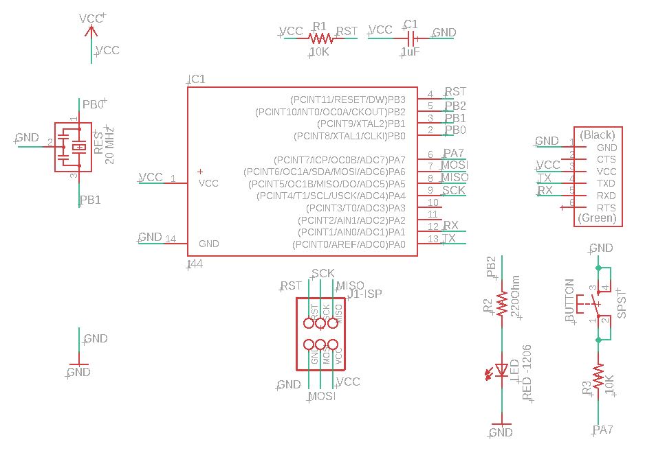
In a circuit all voltage gets used up, and each component offers some resistant that lowers the voltage. Knowing this,
Ohm's law, V =IR, comes in handy for things like figuring out what resistor value to match up with an LED.
LED's have a predefined voltage drop across them and are designed to operate at a particular current value.
The larger the current the LED, the brighter the LED glows, up to a limit. For the most common
LEDs sourced in the fab
inventory, the datasheet
can give us that information. As expected for common LED voltage drop values (~2V), the datasheet gives us a
voltage drop value of 2.4 V. In addition, the datasheet tells us that the specific LED has forward current
equal to 20 mA. Because the surce voltage is 5V and it ends at ground , a total of 5V must drop across
this circuit. Since the LED has a 2V drop, the other 3V must drop across the resistor . Knowing that I want approximately
20 mA to flow through these components, I can find teh resistor value by solving for R:
R = V/I, where V = 3V and I = 20 mA, which gives me 150 Ohm. I will probably choose a slightly bigger value, maybe around 220 Ohm,
which is a common resistor value and still will allow it to sufficiently glow.
A last common check when resistive elements are used is their power rating. Again checking resistors that we source at the fab inventory, tells that their power rating is 0.25 W.
Using the power equation (P = VI) and the predefined voltage (3V) and current values (20 mA) tells me that I'm under
the resistor's rating of 0.25 W. So, I don't have to worry about resistor overheating. It is well within its operating limits.=
Then I added, a a pushbutton switch that hopefully will allow me to interact with the board in real time.Adding a button requires the use of either a pullup or a pulldown resitor. Nearly all digital inputs use a pullup or a pulldown resitor to set the "default" state of the input pin. THey ensure that the button does not create a short circuit between 5V and ground when pressed and that the input pin is never left in floating state. I will use a pullup resistor by connecting the resistor to 5V and by connecting the the other side of the button to ground. In this setup, the input pin will read a high logic value when the button is unpressed and a low-logic value when the button is being pressed.
I designed the PCB in Eagle. All files can be found here:
Here is the schematic:
and here is the board:
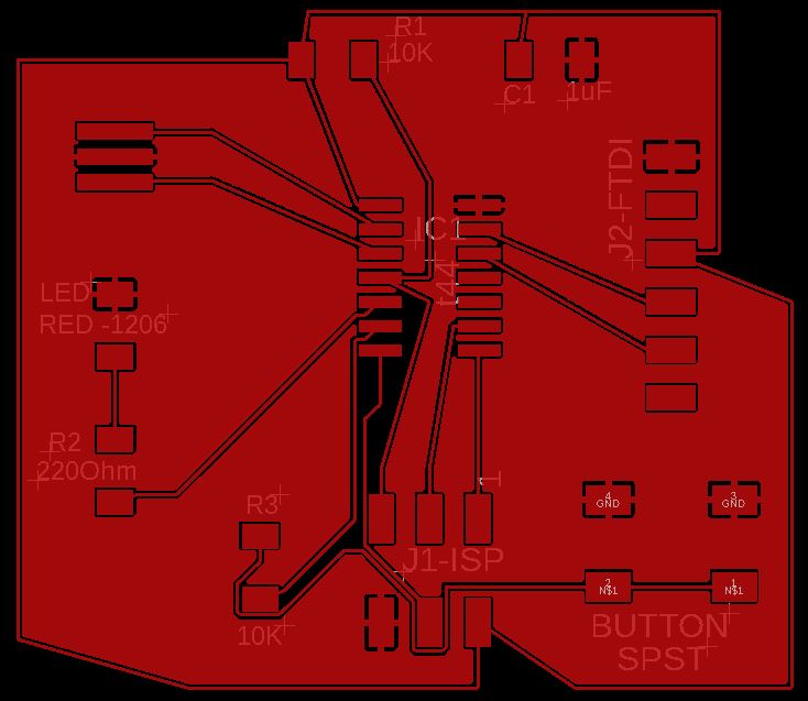
A significant challenge was the routing of all components in the board. Hopefully, the most recent Eagle version version has added some really handy smart interactive routing options that really help the user with the design of single-layer boards. If I have time, I will discuss more about these. In the meantime, here is a link to a very nice webinar by Eagle, Autodesk on these capabilities.