Input Devices
This week’s assignment was to measure something through a sensor. I decided to experiment by adding a phototransistor to a microcontroller board I have designed, using Neil’s board as reference. A phototransistor is a device that is able to sense light levels and alter the current flowing according to the level of light it receives.
Considering Neil’s board example, I have followed the steps done in week 5 to design a new board in Eagle, changing one of its components. Instead of using Attiny45, I used the Attiny44 and did a new board schematic and layout.
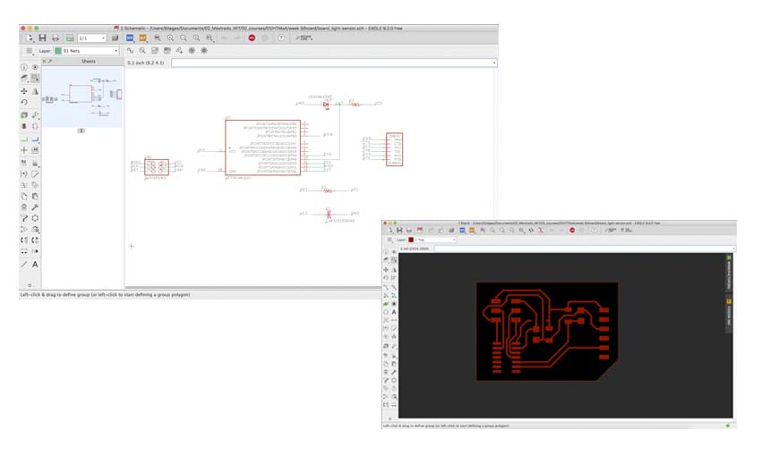
This week I have taken advantage of the possibility of having a bridge in my board, a solution I did not know before, when struggling on week 5, and which was very helpful for connecting two ground parts that were quite hard to match in my design. After milling the board, I got to know that the ideal way of using the bridge is by drawing specific pads for it, for having the wires soldered to. Since I did not know this before, I had my wires soldered directly to the ground plane.
Apparently milling and soldering this week flowed without major issues. To solder the bridge, I have used a coated wire, have exposed its pits using pliers, so that the conductive part could be directly soldered to the board. It was important to solder carefully, since the coating material is a kind of sensitive and can be very easily melted when close to the solder’s heat.
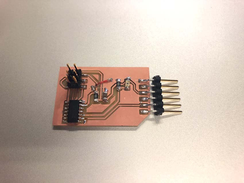
With the board done, I have followed the steps done in week 7 for Embedded Programming, however using specific files and codes to program the phototransistor. As I have taken Neil’s board as an example, I have also referred to his ‘make’ and ‘c’ files. However, since I have changed the board design, changing the Attiny45 for the Attiny44, as well as changing some connections between specific components and their pins, I had to do some modifications on the code.
To begin with, I did the same steps done in week 7:
- connect ISP from the board to the ISP of the usbtiny in the right order using the rainbow cable (check the orientation looking at your board layout)
- using the ftdi cable connect the board to a USBport
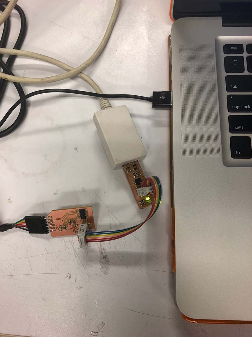
- in your computer create a new folder, I called my phototransistor
- Save both files: c + makefile at your new folder (if using Neil’s code, both are available ate the course website under this week)
- Be sure to rename the makefile file as makefile in case it has any different name
After that, I opened the ‘c’ file and tried to make changes to the code according to the modifications I have done in my board’s design in comparison to Neil’s board. For instance:
Neil’s board:
PBO – MOSI
PA1 – MISO
PB2 - SCK
my board:
PBO – MOSI
PA1 – MISO
PA2 – SCK
However, I could not identify where in the code to make all these changes as well as I did not know where to indicate that I was using an Attiny44 instead of an Attiny45 (and all other possible changes that this component modification possibly implies). The only change I could locate in the code and actually do was the following, also illustrated by the following image:
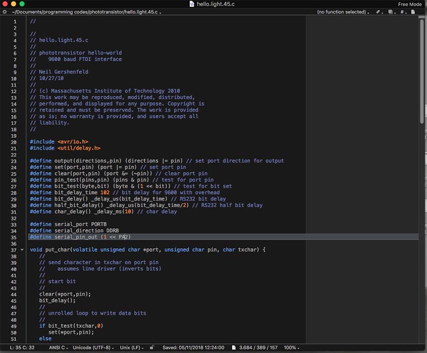
Neil’s port connects to the SCK was the PB2, while in my board the SCK was connected to the PA2. So this was the only possible information I could superfially identify, but still not sure if it is right.
After that, with the gentle help of Agnes Cameron I have tried to check if the board was actually working, using Arduino and Software Serial Library, but we have encountered an error as the following image shows:
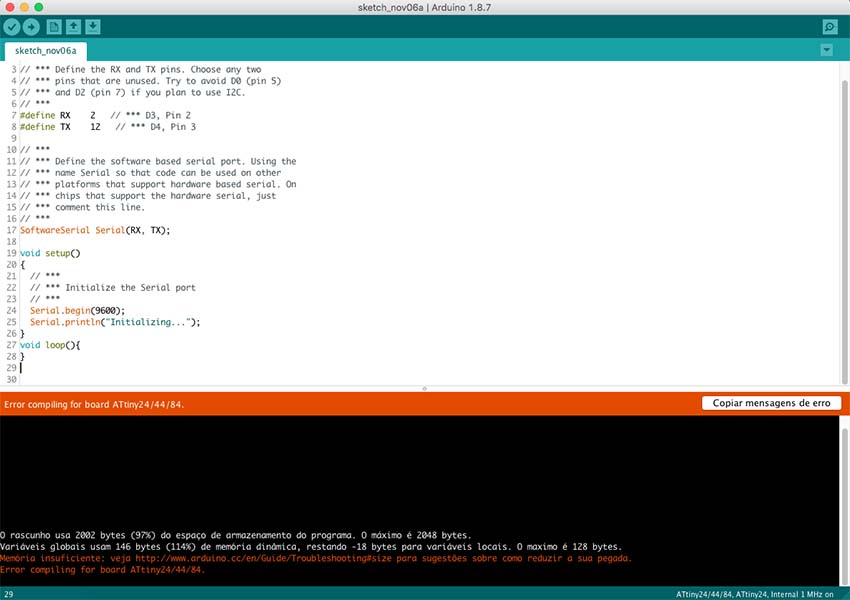
We figured out that I have messed up the pins and assigned MISO and MOSI to pins it was not supposed to when I was doing my schematic.
This week’s assignment was to measure something through a sensor. I decided to experiment by adding a phototransistor to a microcontroller board I have designed, using Neil’s board as reference. A phototransistor is a device that is able to sense light levels and alter the current flowing according to the level of light it receives.
Considering Neil’s board example, I have followed the steps done in week 5 to design a new board in Eagle, changing one of its components. Instead of using Attiny45, I used the Attiny44 and did a new board schematic and layout.

This week I have taken advantage of the possibility of having a bridge in my board, a solution I did not know before, when struggling on week 5, and which was very helpful for connecting two ground parts that were quite hard to match in my design. After milling the board, I got to know that the ideal way of using the bridge is by drawing specific pads for it, for having the wires soldered to. Since I did not know this before, I had my wires soldered directly to the ground plane.
Apparently milling and soldering this week flowed without major issues. To solder the bridge, I have used a coated wire, have exposed its pits using pliers, so that the conductive part could be directly soldered to the board. It was important to solder carefully, since the coating material is a kind of sensitive and can be very easily melted when close to the solder’s heat.

With the board done, I have followed the steps done in week 7 for Embedded Programming, however using specific files and codes to program the phototransistor. As I have taken Neil’s board as an example, I have also referred to his ‘make’ and ‘c’ files. However, since I have changed the board design, changing the Attiny45 for the Attiny44, as well as changing some connections between specific components and their pins, I had to do some modifications on the code.
To begin with, I did the same steps done in week 7:
- connect ISP from the board to the ISP of the usbtiny in the right order using the rainbow cable (check the orientation looking at your board layout)
- using the ftdi cable connect the board to a USBport

- in your computer create a new folder, I called my phototransistor
- Save both files: c + makefile at your new folder (if using Neil’s code, both are available ate the course website under this week)
- Be sure to rename the makefile file as makefile in case it has any different name
After that, I opened the ‘c’ file and tried to make changes to the code according to the modifications I have done in my board’s design in comparison to Neil’s board. For instance:
Neil’s board:
PBO – MOSI
PA1 – MISO
PB2 - SCK
my board:
PBO – MOSI
PA1 – MISO
PA2 – SCK
However, I could not identify where in the code to make all these changes as well as I did not know where to indicate that I was using an Attiny44 instead of an Attiny45 (and all other possible changes that this component modification possibly implies). The only change I could locate in the code and actually do was the following, also illustrated by the following image:

Neil’s port connects to the SCK was the PB2, while in my board the SCK was connected to the PA2. So this was the only possible information I could superfially identify, but still not sure if it is right.
After that, with the gentle help of Agnes Cameron I have tried to check if the board was actually working, using Arduino and Software Serial Library, but we have encountered an error as the following image shows:

We figured out that I have messed up the pins and assigned MISO and MOSI to pins it was not supposed to when I was doing my schematic.