Electronics design
To mill my own Hello World circuit, I performed the following steps (done on Linux using KiCad) :
- Install the KiCad software and fab libraries (from the course website). The two fab libraries are databases containing parameters and physical dimensions of the components in our fab lab. (See below for installation instructions.)
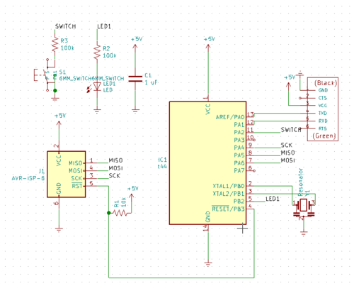
- Open schematic view.
- Lay down the logical network structure, including wire labels for convenience.
- Set the components' parameters (resistance level, capacitance, etc.)
- Set the footprints of the components.
- Annotate the circuit, which gives unique names to each component.
- Export the circuit as a netlist.
- Open PCBView. Import the netlist.
- Set trace and grid parameters. (Make the traces a bit wider than default. Make the separation between traces a bit wider than default. Make the grid finer than default.) Set global design rules by Setup > Global Design Rules.
- Move the components around into a configuration where everything can be connected to everything else w/o traces overlapping each other. (Sketching on paper or referring to previous years' projects. http://fab.cba.mit.edu/classes/863.17/Architecture/people/ehoseini/week5/index.html)
- Draw traces, making sure to space them apart. (To avoid future problems where a drop of solder causes a short circuit.)
1 Experiences with circuit design
Throughout, I gathered bits of advice for how to do the design process:
- The KiCad software is essentially a federation of separate programs (like an office software suite). The flow is that you design the logical layout of the connections, then export those connections as a netlist, then import the netlist into a second program for spatially laying out the PCB board.
- You must import fab libraries into the schematic and PCB programs separately.
- The initial circuit layout has no meaningful geometry. In particular, the pins are in arbitrary positions. All that matters is what is connected to what.
- As a result, getting the exact components doesn't matter as long as the footprint is correct.
- Components are initially given automatic names with question marks in them. The "annotate net" eliminates all the ? labels. For example, it turns resistors R? R? R? into R1 R2 R3.
- Pro tip(!) : To reduce the number of wires, you can add power symbols or labels to wires. All same-labeled components will be considered connected.
- Our microcontroller for this project is ATTiny44A-SSU
- Many circuit elements are of type 1206, which I believe refers to their dimensions.
My logical layout worked like this:
- Assign PCB symbols
- capacitor SMD (surface mount) hand solder 1206
- 6 pin connector ConnectorPinHeader 2x3 2.54mm SMD
- 1206 gives dimensionality of small parts, including resistor and capacitor.
- Resistor: 1206
- Design rules: set clearance and track width accordingly. (units in mm)
- Grid settings are in dropdown on toolbar, not in a menu
- When exporting, be sure to export only Front copper (it's a one-sided board) and to export only the board area, not the whole page.
- If you have the misfortune of using LibreOffice Draw to view SVG objects, note that it doesn't render joins between lines properly — the lines look disconnected. This is a problem with rendering, not with the drawing — opening in a suitable program such as Inkscape solves the problem.
- You must draw the outline of the board. To do so, select the Edge.Cuts layer on the right hand side of the screen. Then draw a polygon (square). The square should be unfilled.
- To delete all traces ("rip up"), select all and look under the Edit menu.
- http://fab.cba.mit.edu/classes/863.17/Architecture/people/ehoseini/week5/index.html
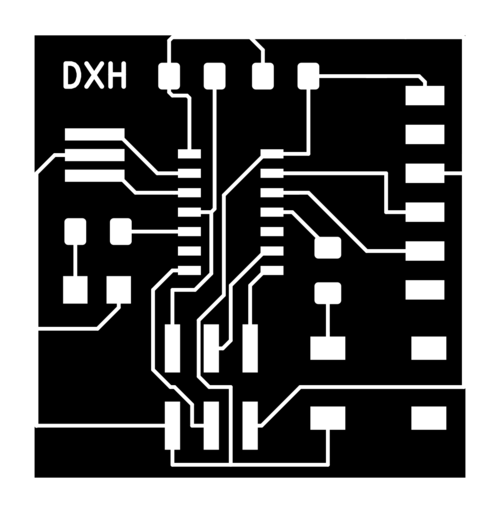
My initial PBC layout ended up with traces too narrow and too close together.
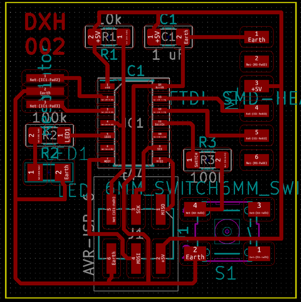
After adjusting the global design rules to increase trace width and separation (0.4), my improved (#002) circuit looked like this:
The following script converts an SVG as exported by KiCad into a 1000 dpi png image with inverted black/white colors. It generates the traces and the border image from the same SVG. Importantly, the traces image will have a white border than needs to be converted to black.
convert -density 1000 h.svg -color Black -border 8%x8% h.png && convert h.png -negate h_traces.png
convert -density 1000 h.svg -fx 0 -alpha off  -bordercolor White -border 8%x8% -negate h_border.png
2 Programming
I was also able to experiment with some programming! I used the
program picocom to present a serial interface to the board. Here's
what I learned:
To be run only once, when you first build the board (to set the clock rate)
make avrisp2-fuses
To be run each time you want to download a new program:
make avrisp2
This Makefile compiles a c file (the PROJECT variable in the makefile) into attiny code and downloads it onto the machine. The target changes depending on what the programmer is. avrisp2 is the small blue box one.
misc command:
avrdude -p t44 -c avrisp2 -v
Install picocom.
sudo picocom -b 115200 /dev/ttyUSB0
-b is baud rate (as listed in the echo hello world c program).
Apparently the button has convention 0 = pressed, 1 = unpressed.
C-a C-x to exit picocom.
- Registers are named after pins (A0, A1, B0, B1, etc.)
- Two registers important for writing. To write to port a, two registers:
- DDRA tells each pin whether each pin is an input or output. ("DIRECTION")
- PORTA defines the output states of the output pin.
On inputs, PORTA tells input pins whether to float (0) or not (1). You might want an input to float if connecting to a capacitative element e.g. touch-capacitance.
I modified the initial echo hello world program to do several other things with the LED. I changed the main loop as follows:
#define led_port PORTB
#define led_direction DDRB
#define led_pins PINB


while (1) {
     dxh_i ++;
     // PROGRAM 1: flicker
     /* if(dxh_i > dxh_freq) { */
     /*   dxh_i -= dxh_freq; */
     /*   dxh_led = 1-dxh_led; */

     /* } */
     // clear(led_port,(1 << PB2));
     // set(led_port, (dxh_led << PB2) ); // current state.

     // PROGRAM 2: dimmer
     // clear(led_port,(1 << PB2));
     // set(led_port, (((dxh_i % 2)==0) << PB2) ); // current state.


     // PROGRAM 3: led is on unless you press button
     clear(PORTA, (1 << PA2));
     clear(PORTB, (1 << PB2));
     PORTB |= PINA;
}
(!) One important obstacle was I needed to use uint32_t for large
integer variables like the frequency (250000) and the counter variable
dxh_i. When they were initially integers, the code could not work.