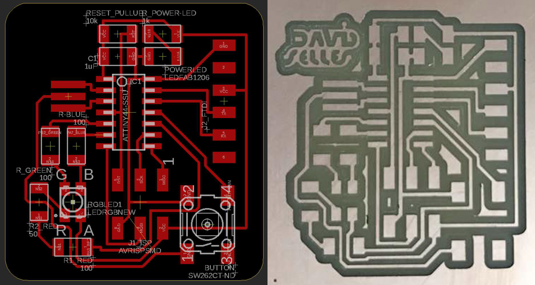
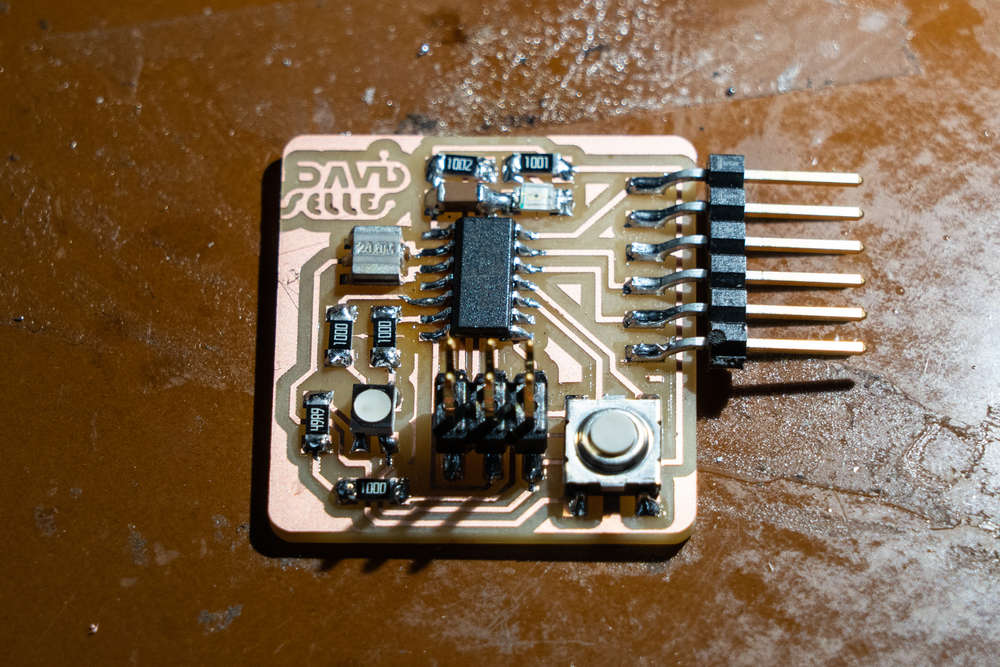
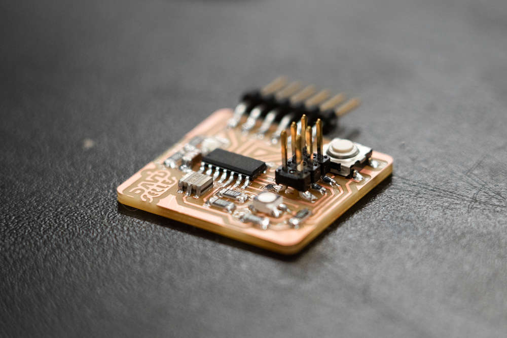
I decided to use Autodesk Eagle to design my board, mainly because I already use Autodesk Fusion and because a number of my classmates were using Eagle as well.


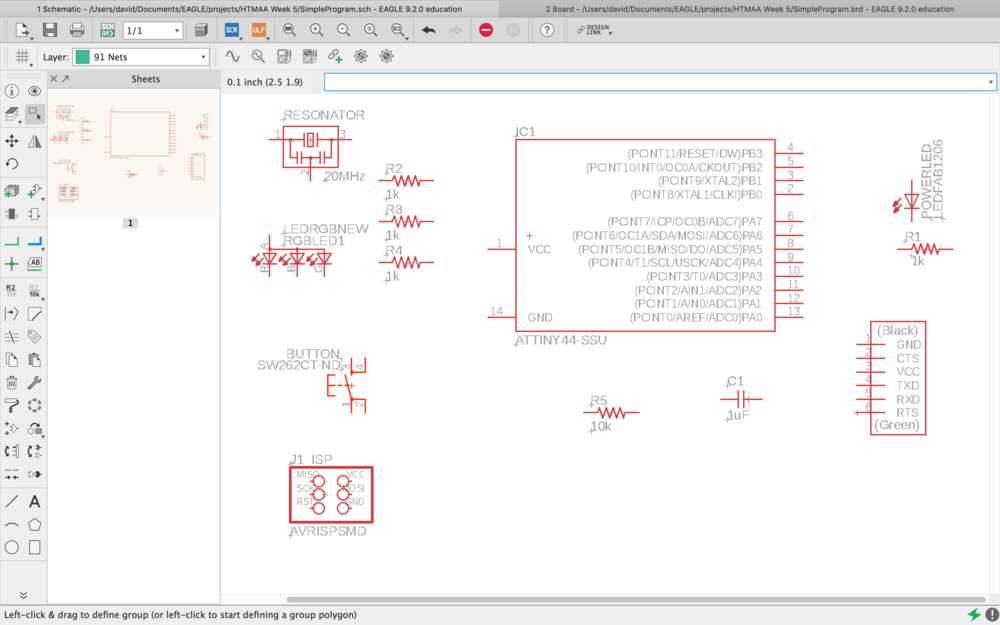
One of my classmates Victoria Shen happened to leave some of her work around the lab which proved to be a helpful starting point, if for nothing more than to see how these parts are named in the fablab Eagle library.

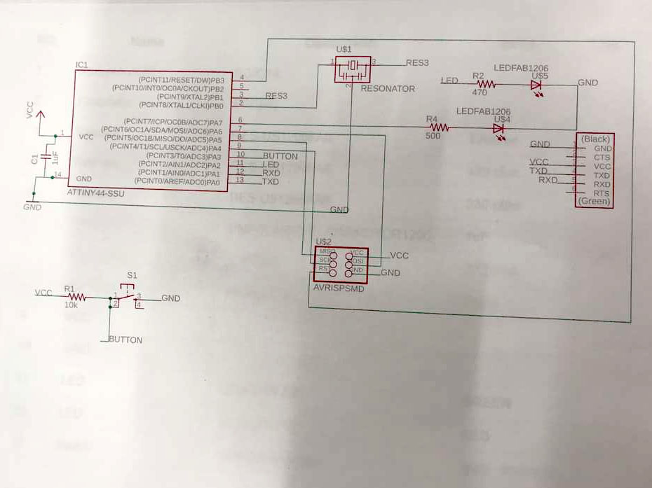
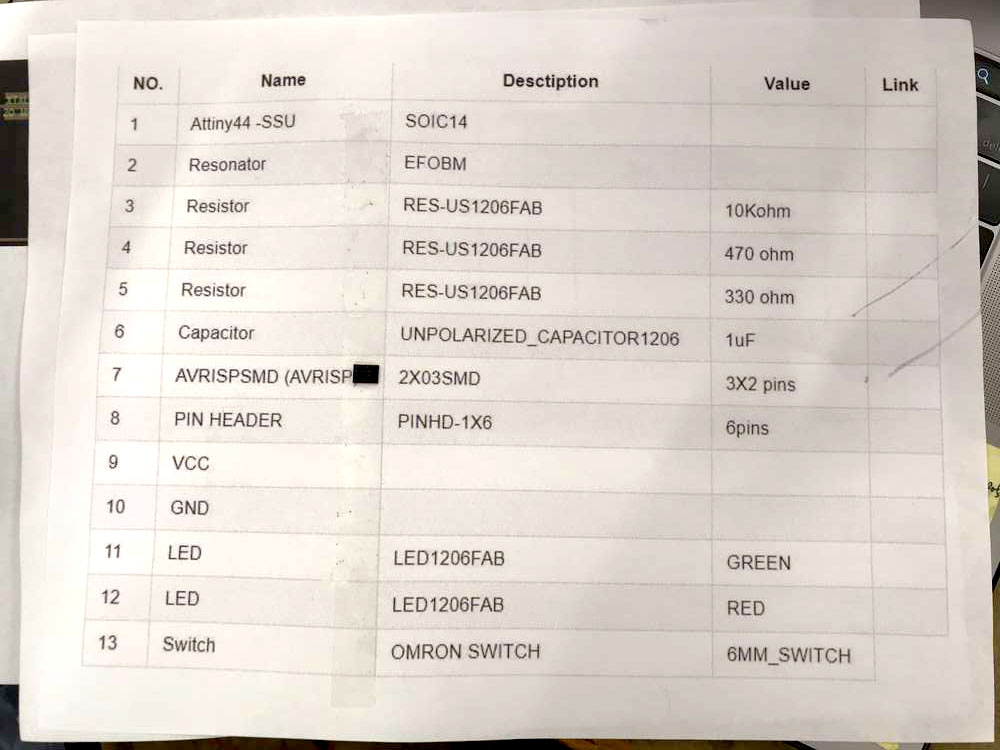
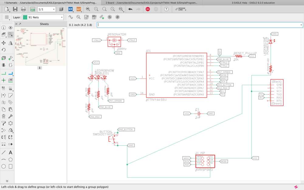
I was able to find the parts in the fablab library without too much trouble. Along the way I referenced some online tutorials on how to label and name components and net stubs in order to make connections between parts and to keep the document looking clean (see helpful links section up top).

Connecting everything together wasn't too challenging, though it's tricky to spatially plan at this stage. While this net would work, I ended up needing to switch around some of the pin connections between my new components since these initial positions didn't lend themselves to optimal physical placement.

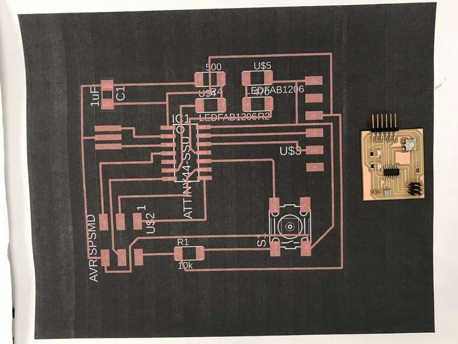
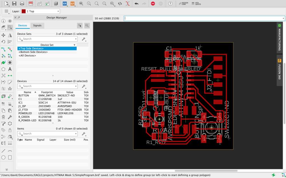
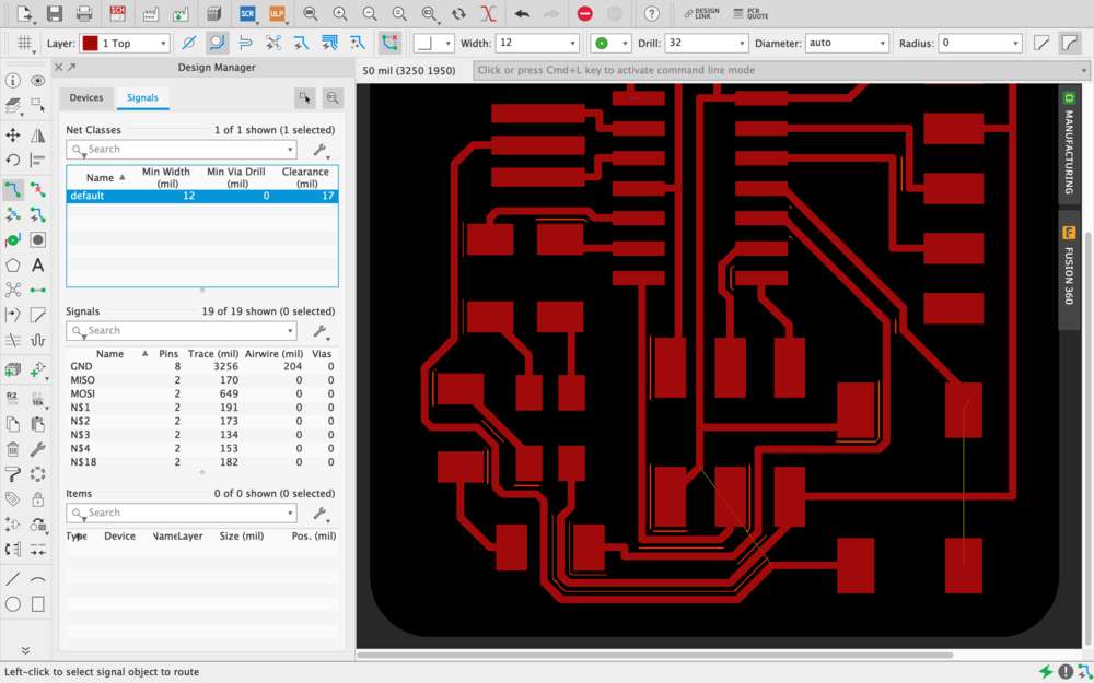
Routing everything was the most time consuming part of the design phase. I used Neil's board as a starting point for my own, and did my best to plan around what already existed. I ended up using my button as a bridge to help cross signals from the right side of the chip to the left side of the board.

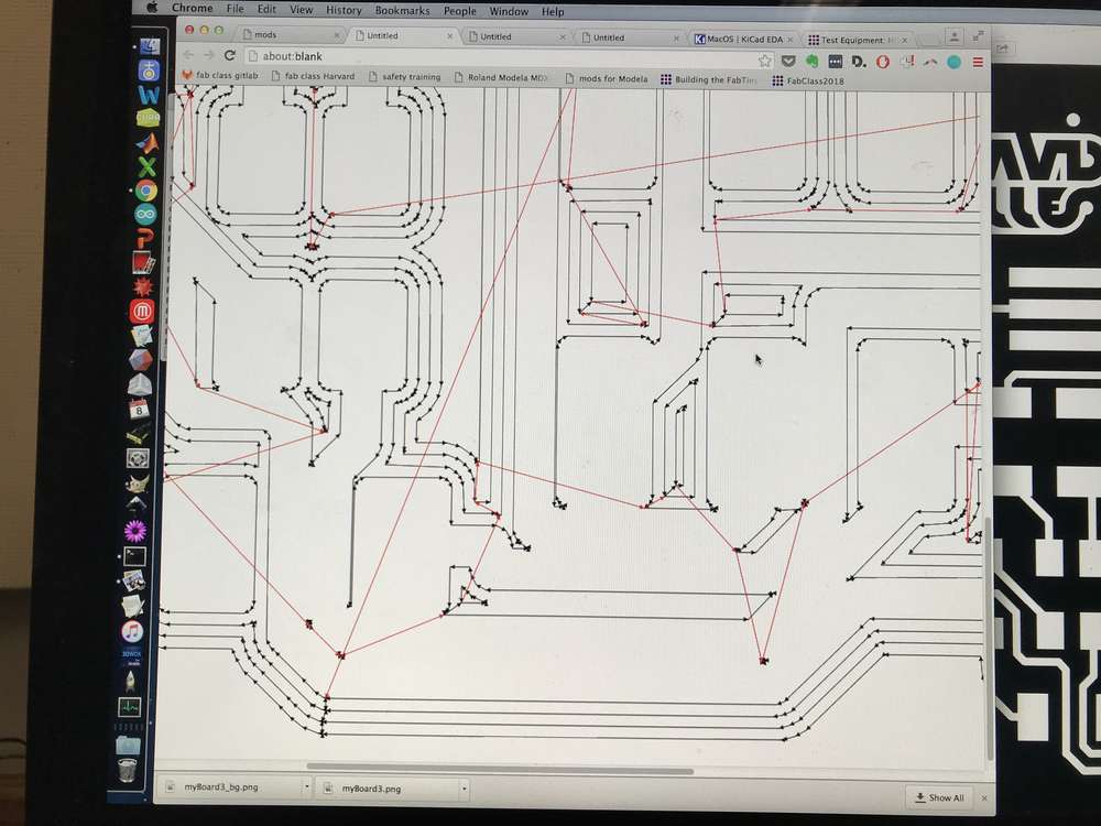
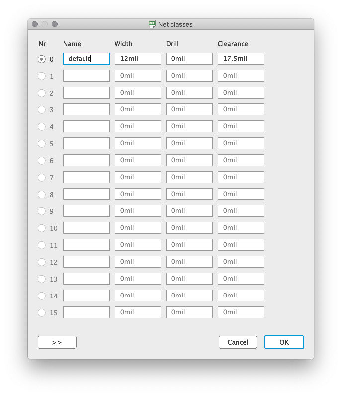
Unfortunately my traces were too close together, and ended up getting merged when I was about to mill my board. Through some trial and error I found that giving my traces a clearance of about 17.5 or 18 mils was enough to ensure adequate separation. It's possible to set this up using the Net Classes options dialog, at which point the display will visually signal when traces are too close together.


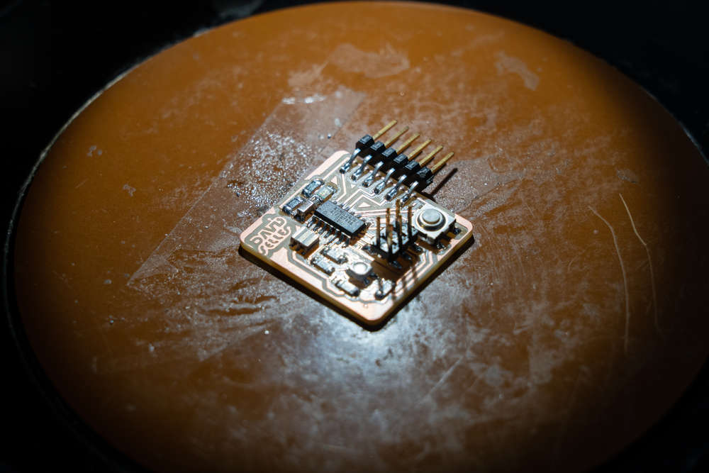
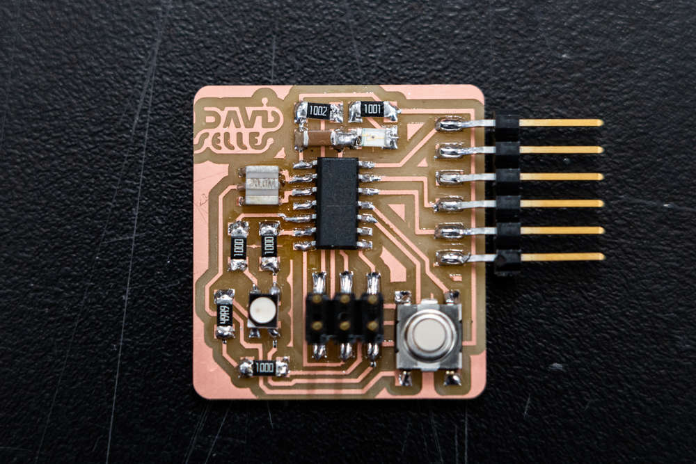
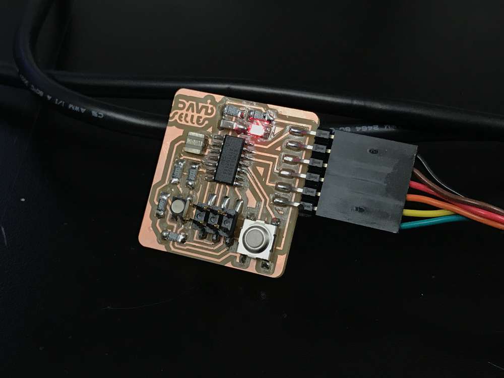
Finally the board was ready, and I was able to mill it out. For kicks, I added a personal touch in some open space in the upper left corner, using a personal logo I'd previously made in Illustrator. It was easy to incorporate once I exported the traces from Eagle.
I should note, however, that exporting images for production from Eagle is non-trivial. All other non-printing layers need to be hidden. After some searching online, I found the command display none top, which first hides all layers, then selectively shows the top traces. I was able to get everything back by typing display last.
