PCB Milling
This week's PCB design was prescribed, but soon enough we'll be designing our own. The programmer we make this week can be used to program all of our subsequent boards, so I was looking forward to seeing this week through. We used a paper-based composite plate plated with copper (about 0.004" thick) on one side. Once cut away, the copper forms the traces for the circuit.
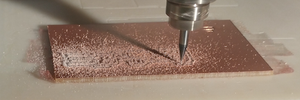
Harvard has two small-scale milling machines in its fab labs. They are similar to the vinylcutter in operation and we used Neil's browser program, mods, for both, adjusting depth of cut as necessary. The milling machines use two different cutting tips, a 1/32" blade and a 1/64" blade, for cutting the board's outlines and traces, respectively.


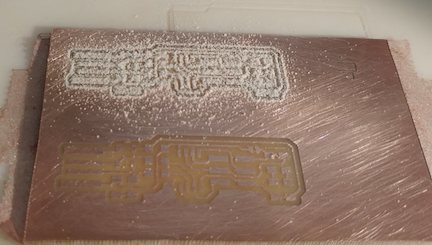
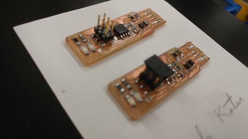
The design for this board had already been exported into black-and-white PNG files that were posted on the course website. We were able to import these into mods and populate successful boards without making any modifications to the design. The finicky parts of this assignment were determining an effective cut depth, one that didn't leave copper outside of the traces but didn't dig into the board too deeply, and soldering components on correctly. I found that the default cut depth for the board outline was very workable - it cut through the board without cutting into the sacrificial layer of plastic on the machine bed too deeply. The default cut depth for the trace cut didn't quite cut through all of the copper on my board, so I adjusted it to 0.01", which proved perfect. The board was definitely not completely flat on the machine bed, as evidenced by the uneven copper surface left after the too-shallow trace cut. I made two copies of the USBtiny board and populated each with components.
Soldering proved fairly straightforward for me. I used the magnifying apparatus on the lab bench to see small components more clearly and to make sure that no unintended connections were made with stray solder. I used a lab PC and working USBtiny to program one of my boards and then used this one to program the other.
