This weeks assignment was to create the Echo Hello World board from scratch using Eagle and then fabricate it.
I first wanted to draw out the circuit by hand based on the picture given to us on the FAB website to understand how all of the different parts fit together. In addition to the existing board, I also had to add a button and an LED to the circuit, making sure I also added pull-up resistors accordingly. Pull-up resistors are very common when using microcontrollers (MCUs) or any digital logic device.
Let's say you have an MCU with one pin configured as an input. If there is nothing connected to the pin and your program reads the state of the pin, will it be high (pulled to VCC) or low (pulled to ground)? It is difficult to tell. This phenomena is referred to as floating. To prevent this unknown state, a pull-up or pull-down resistor will ensure that the pin is in either a high or low state, while also using a low amount of current. With a pull-up resistor, the input pin will read a high state when the button is not pressed. In other words, a small amount of current is flowing between VCC and the input pin (not to ground), thus the input pin reads close to VCC. When the button is pressed, it connects the input pin directly to ground. The current flows through the resistor to ground, thus the input pin reads a low state. Keep in mind, if the resistor wasn't there, your button would connect VCC to ground, which is very bad and is also known as a short. Lastly, you want a resistor value on the order of 10k Ohms for the pull-up.
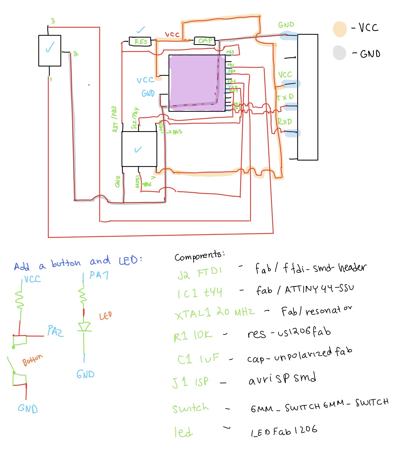
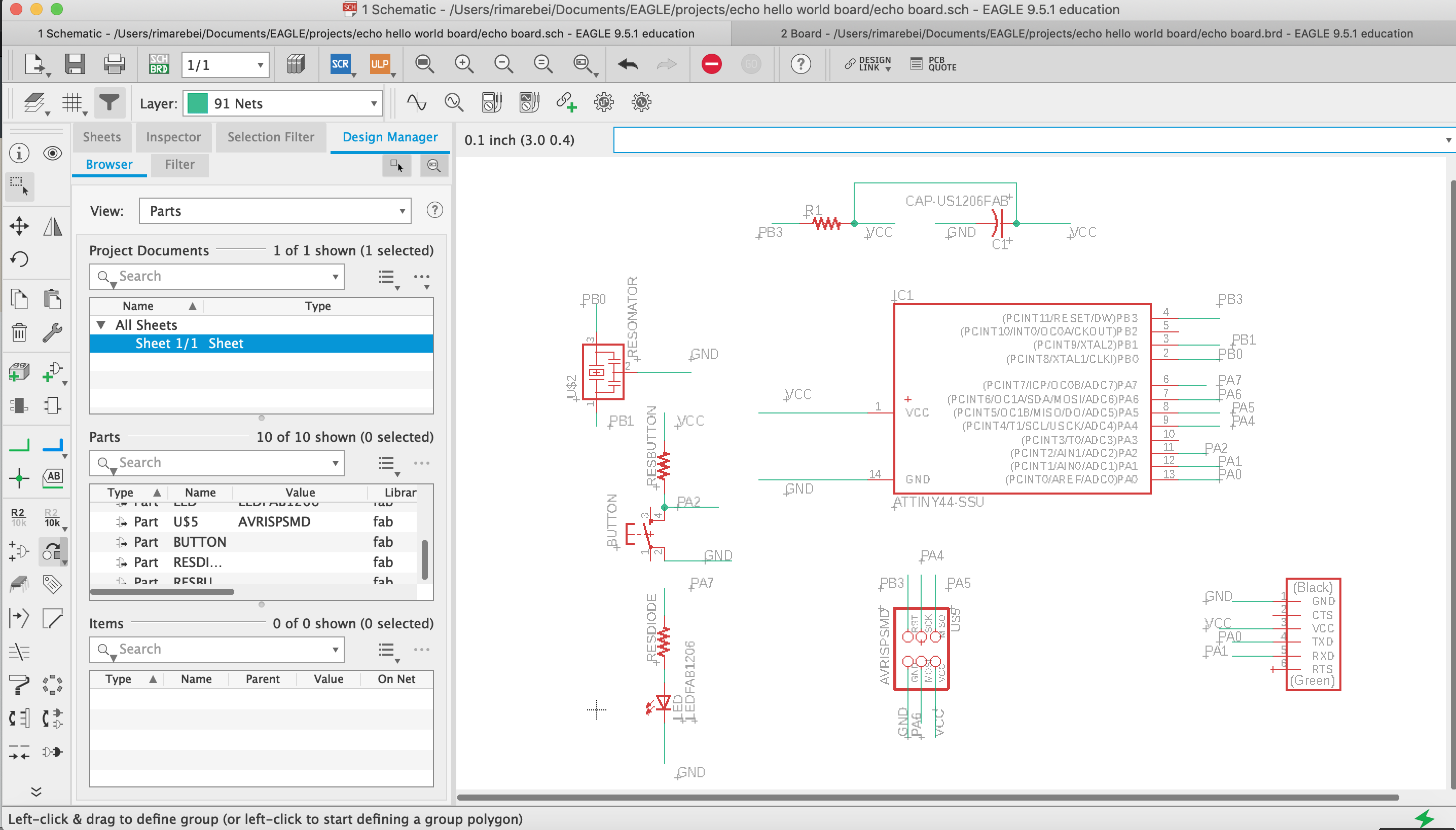
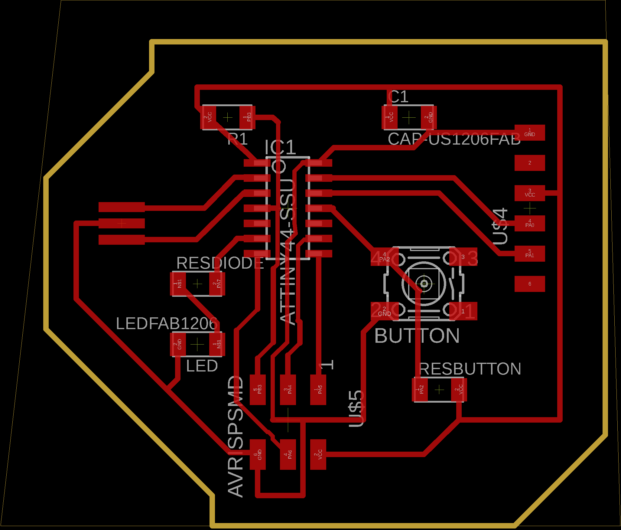
This was my first time ever using Eagle! I created a project and then created a schematic within the project. I first had to import the fab.lbr file provided to add the fab lab components to my Eagle library and to make sure I was using the correct footprints for the parts we have available to us. When creating the schematic, the circuit that I drew really helped me visualize what parts connected to what.
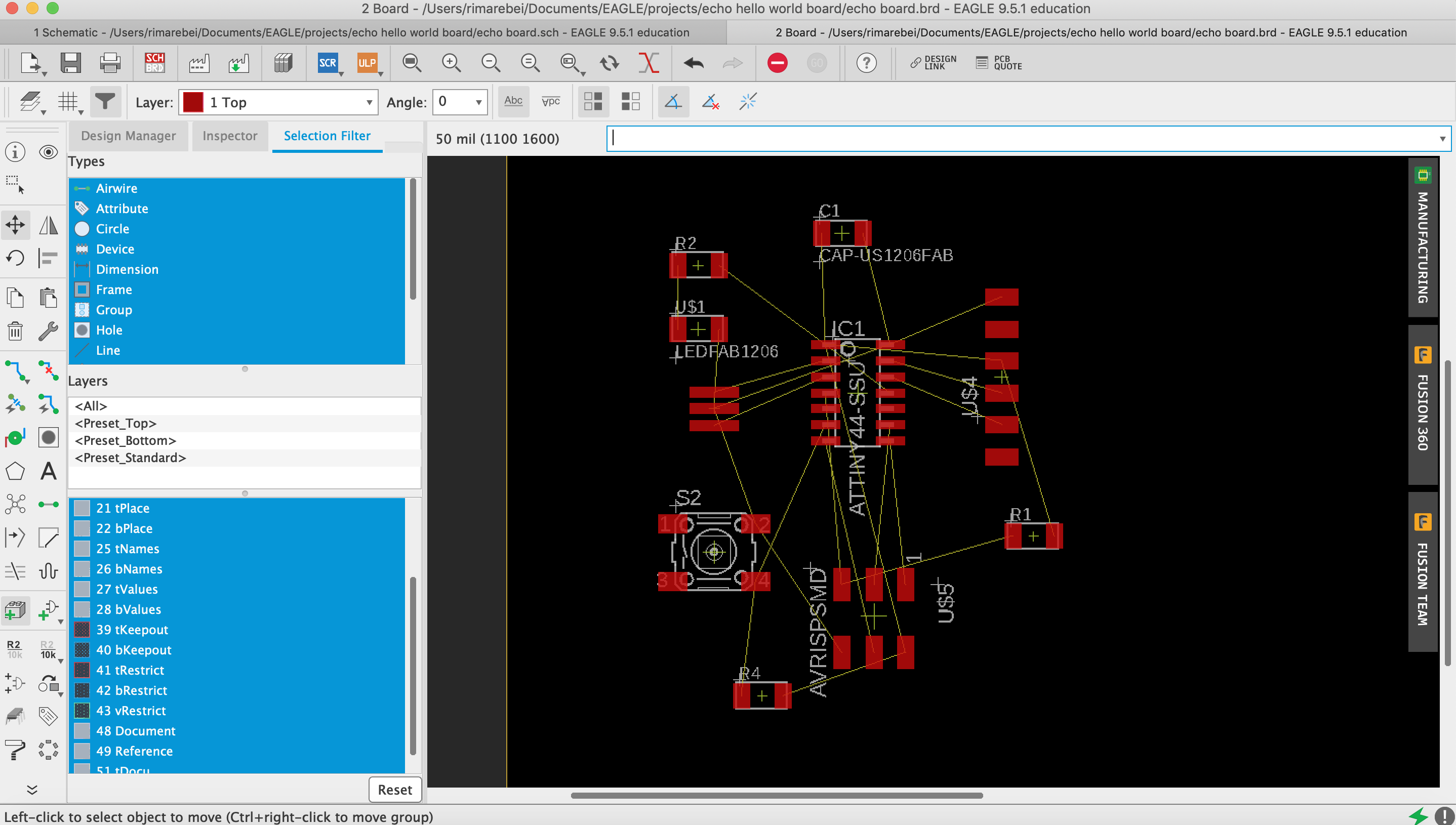
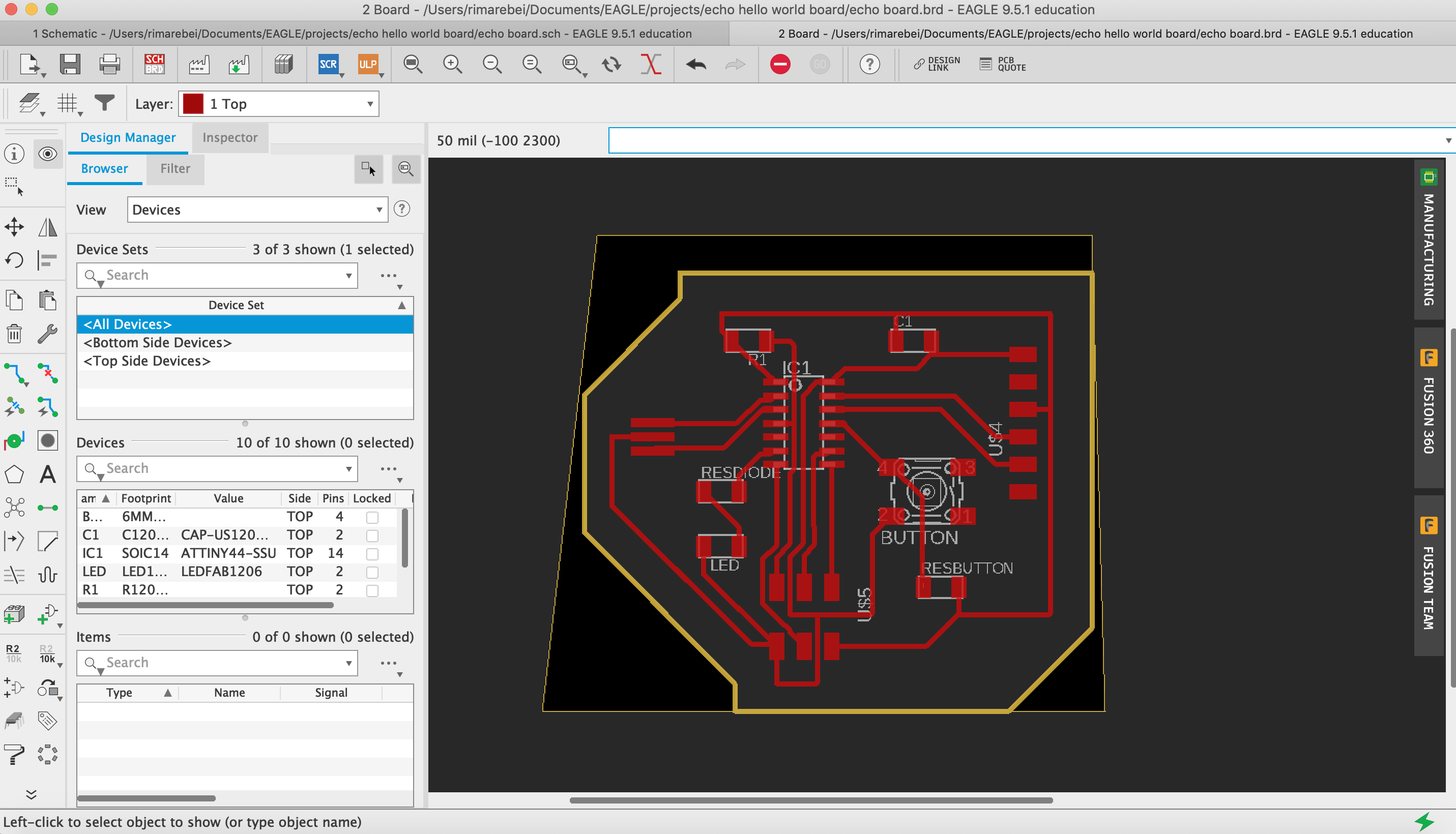
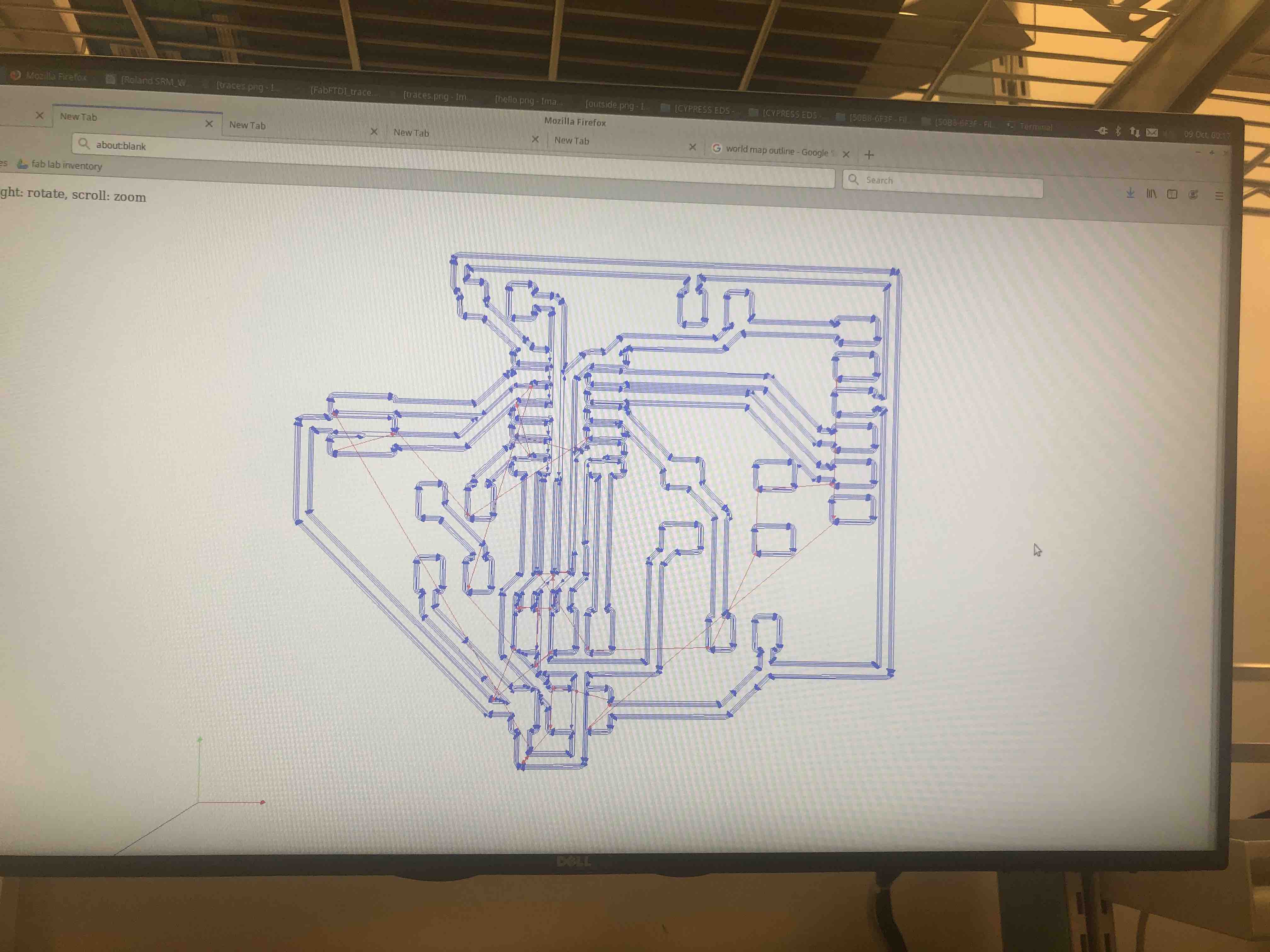
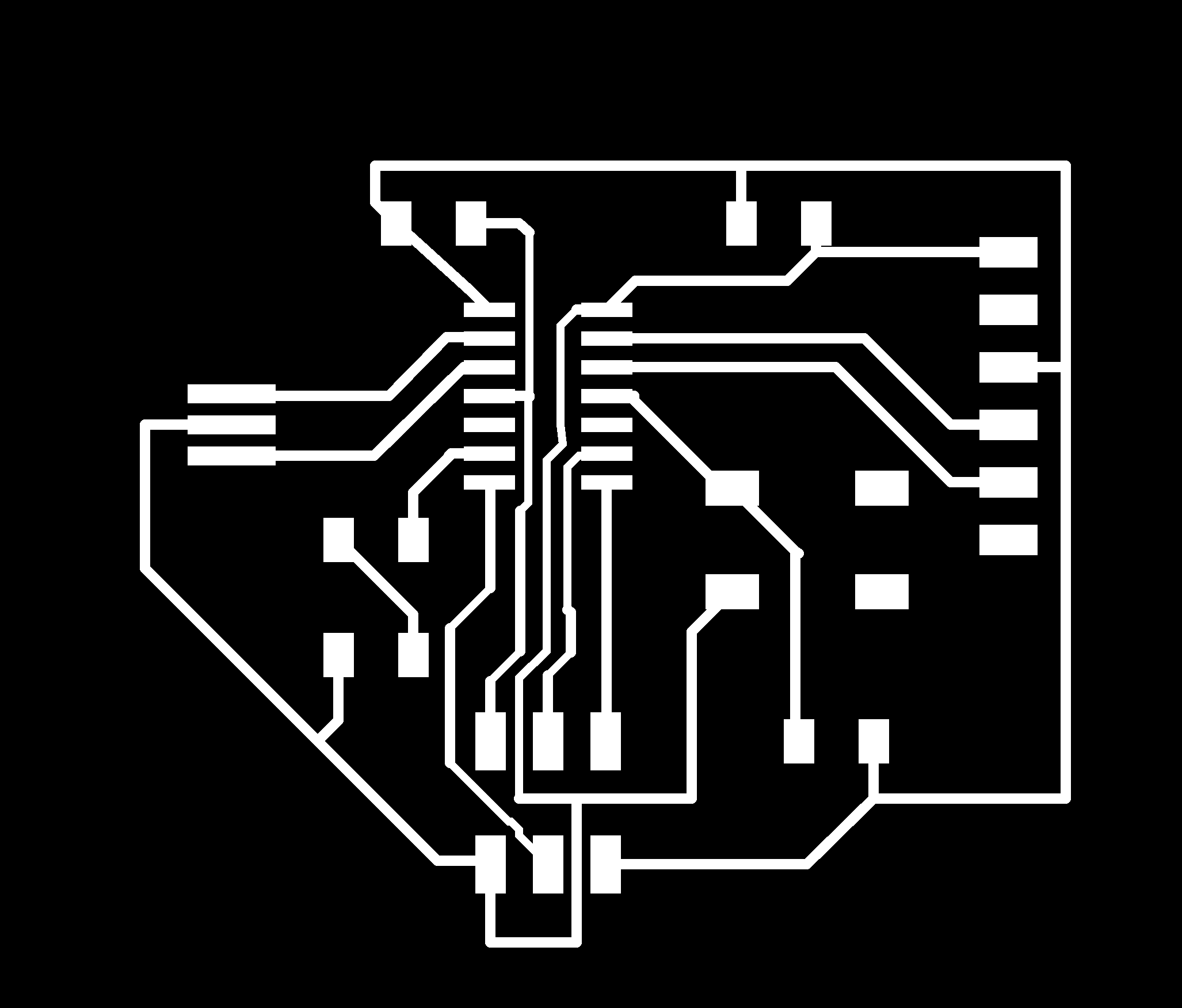
The next step was to create the traces. All I had to do to start the board was click the "Generate/switch to board" button on the top of the screen. I found this a little difficult because I was so confused by all of the yellow lines everywhere and how they should all connect. It seemed like it was a puzzle and I had to find the best place where each component would lay on the board and the best possible traces between them. After figuring out all of the connections, I had to make sure that the board was able to be milled by at least the 1/64th in. drill bit. In order to make sure about this, I set the grid to 10 mil and made sure there was enough room between each trace based on the grid and moved hte traces accordingly. Also, all of my trace width was .16 mil.
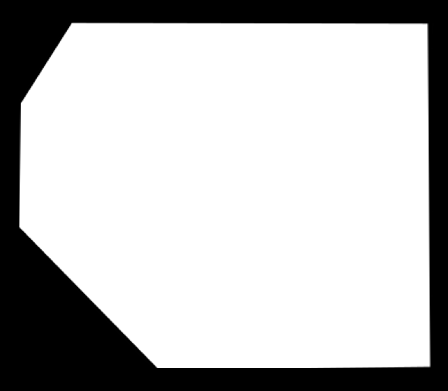
After arranging all of the components, I needed to make an outline for the board. I didn't know that I could just drag the already existing thin yellow lines so I changed the layer in EAGLE to top and drew a yellow border around my board. I wasn't really sure what that did because then when I tried to export the board to PNG images the border did not work out.
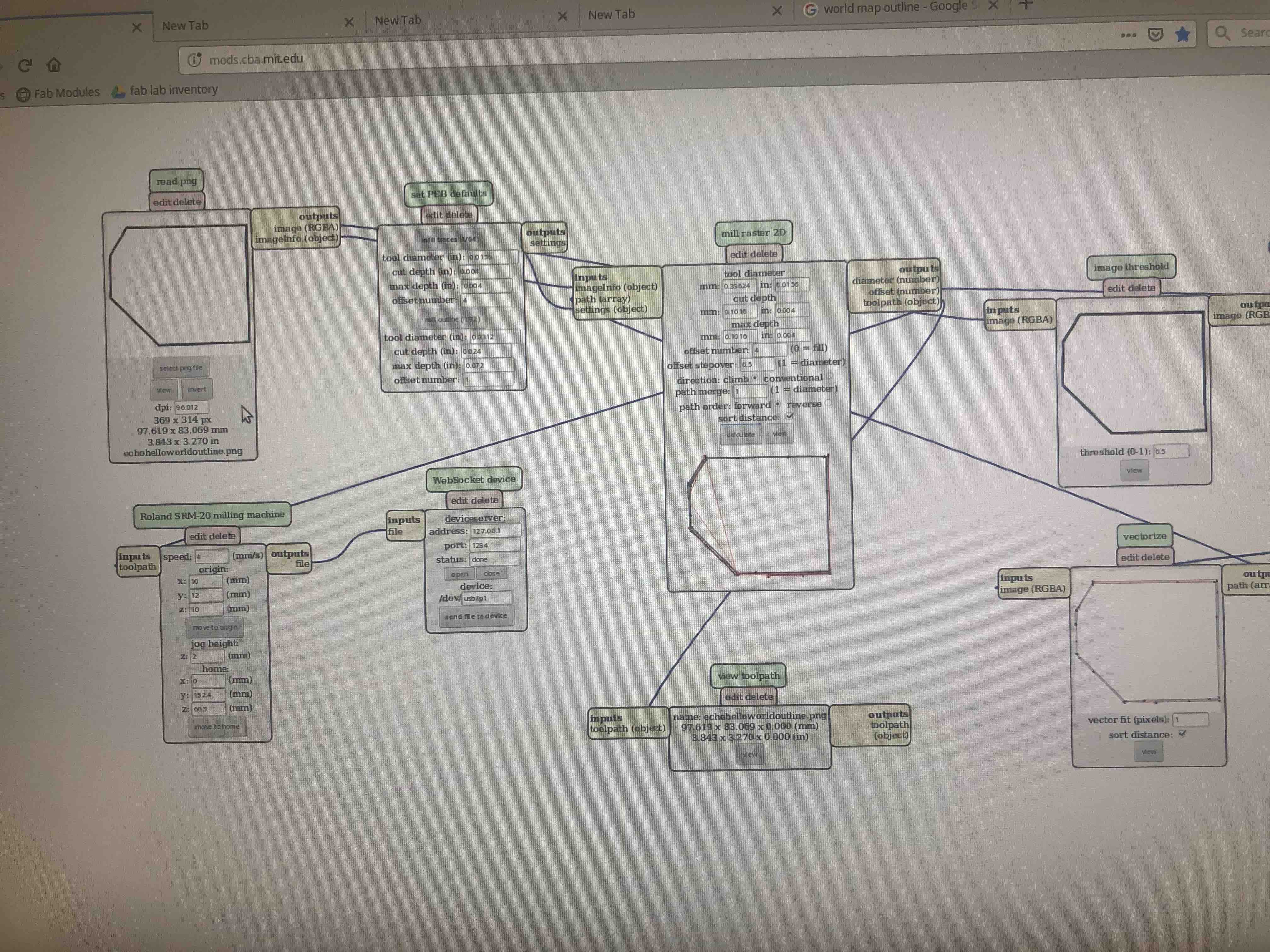
After hours of trying to figure out the outline of the board, I wasn't able to so I decided to make my own png image of the board outline using Inkscape and try to match up with the board using the CBA module for the Roland machine. As you will see, it didn't work out great.
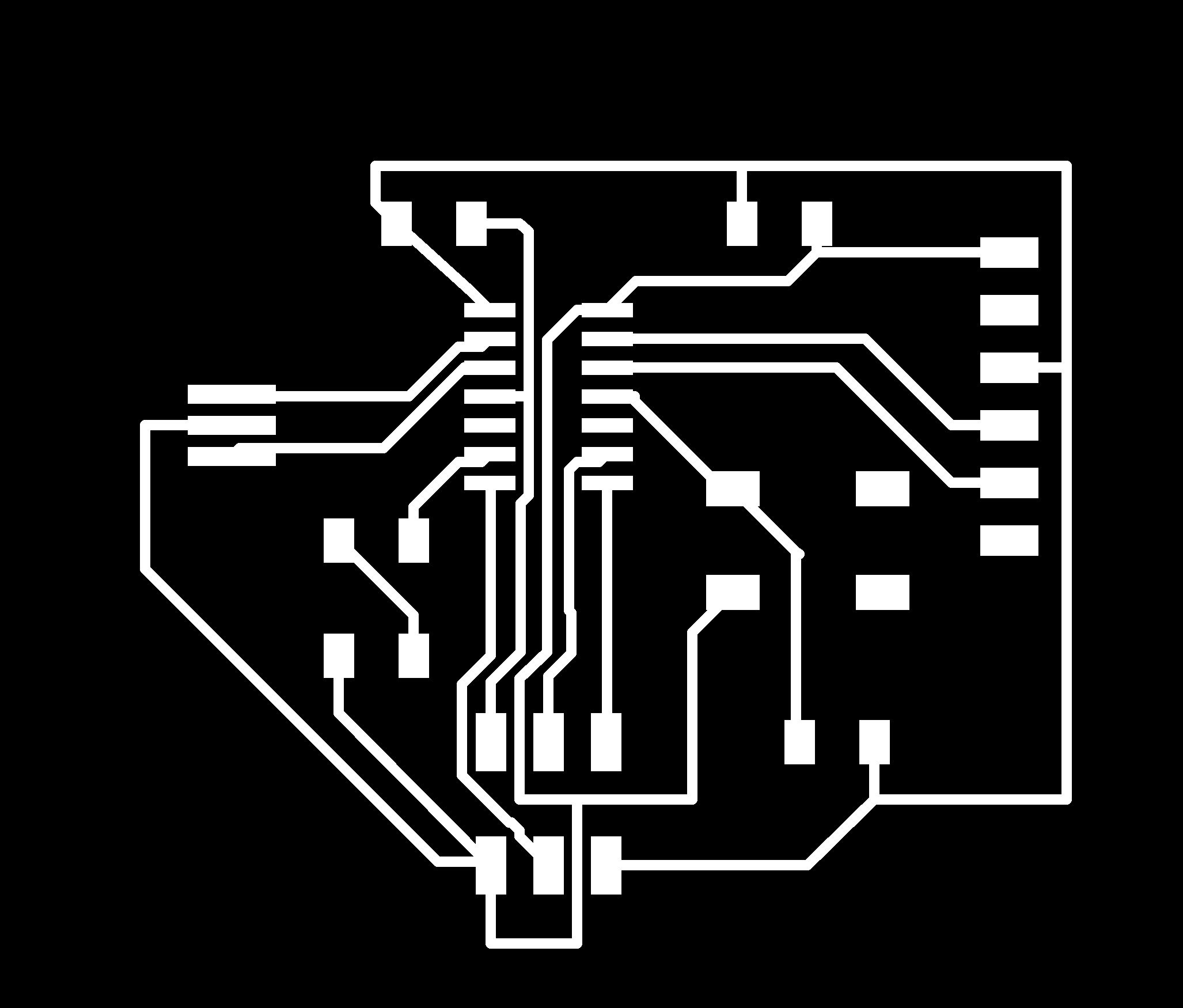
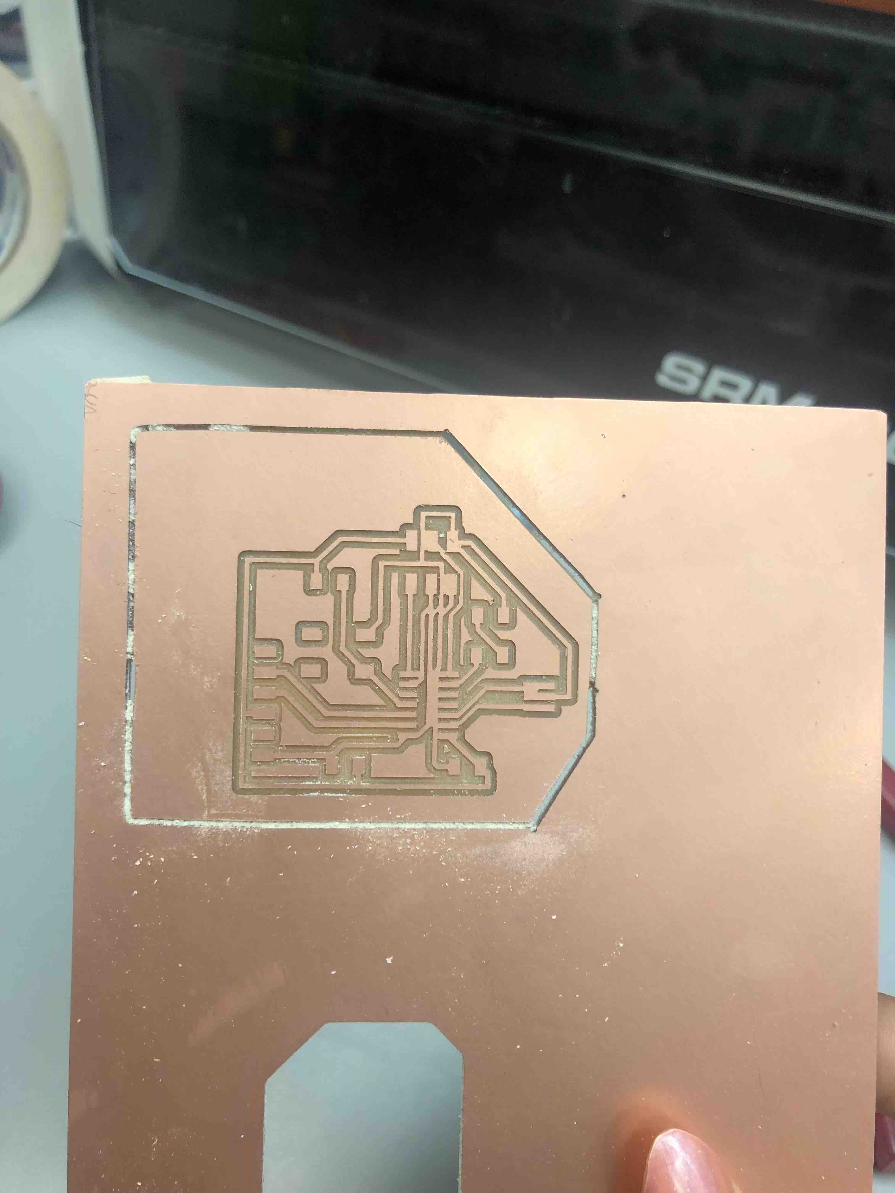
I uploaded the traces file and starting milling that board. I thought that went well however after I vacuumed the board I saw that a lot of traces were not cut properly. However, I decided I might as well use this board and use it as a practice board and finish milling the border aswell.
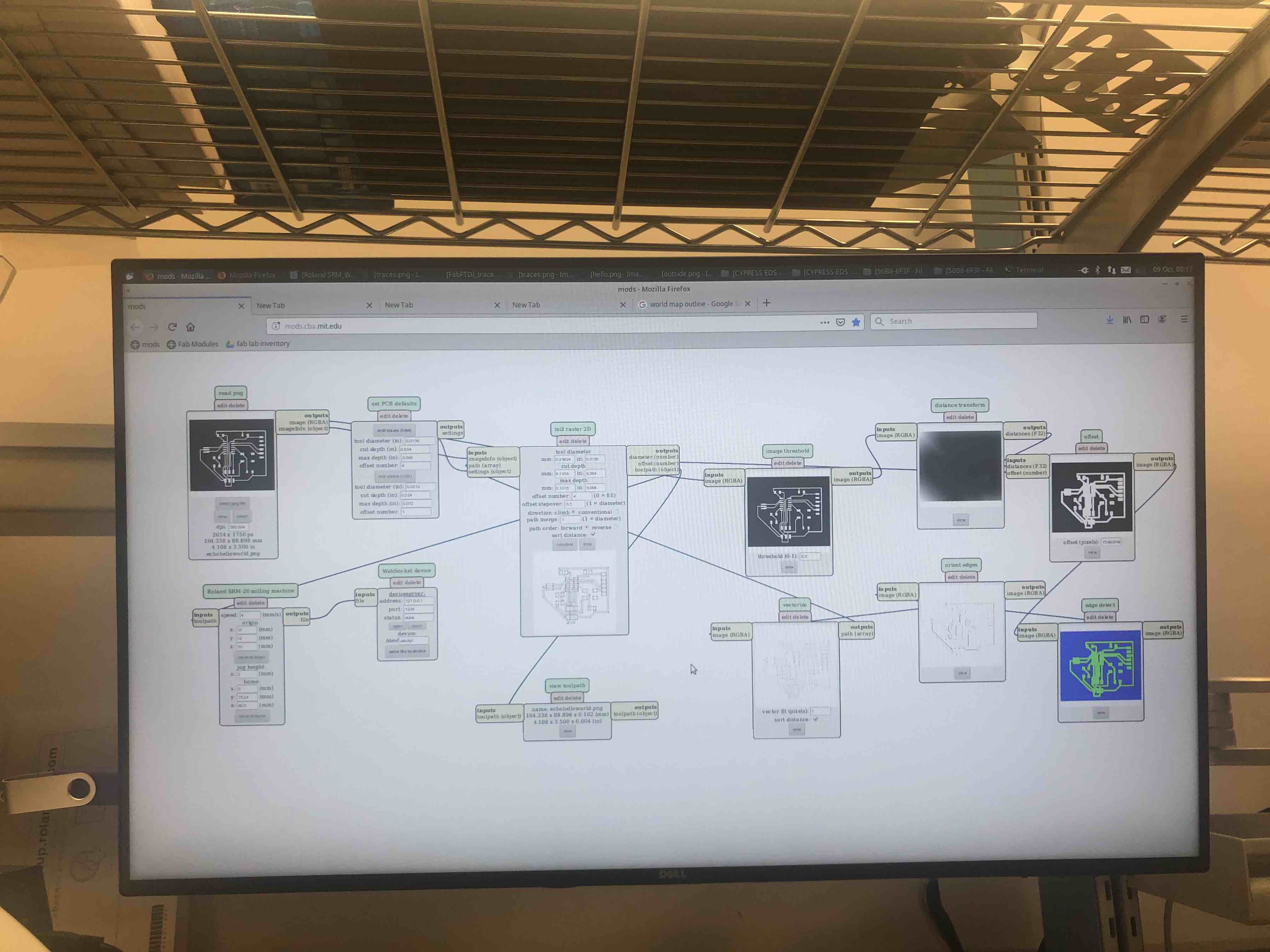
One big problem of creating the outline of the board seperatly was that I had a really hard time figuring out the correct dpi for the outline and where to make the origin of the cut aswell. This whole process to an increadibly long time and at the end of the day, pretty much came down to luck. I tried measuring how big I thought the traces were and tried to make a dpi number accordingly.
Overall, this board had many issues, from the traces to the outline that I had to completly redo it from scratch.
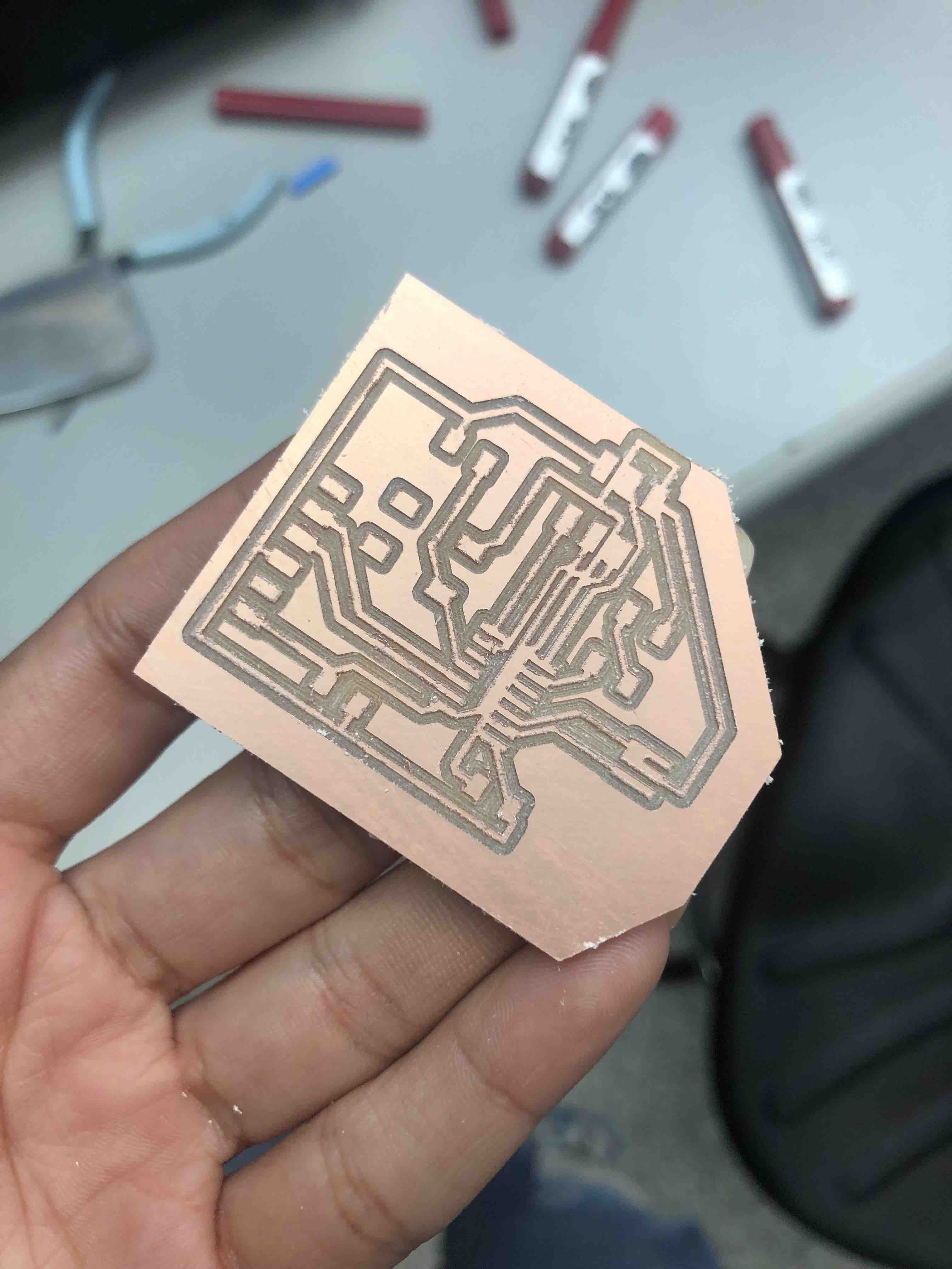
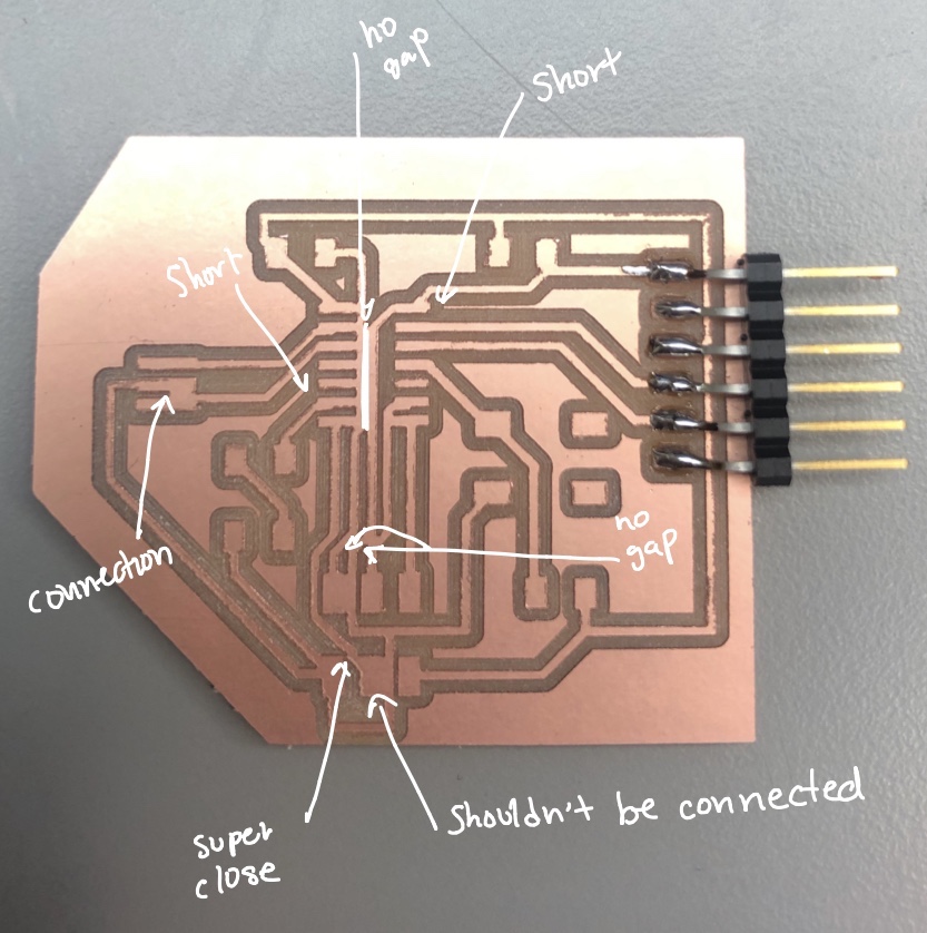
I went back to Eagle and made sure all my traces had enough room between them to that the machine could drill through them to fix all of the problems from the pictures above and finally got a good final result with a board.
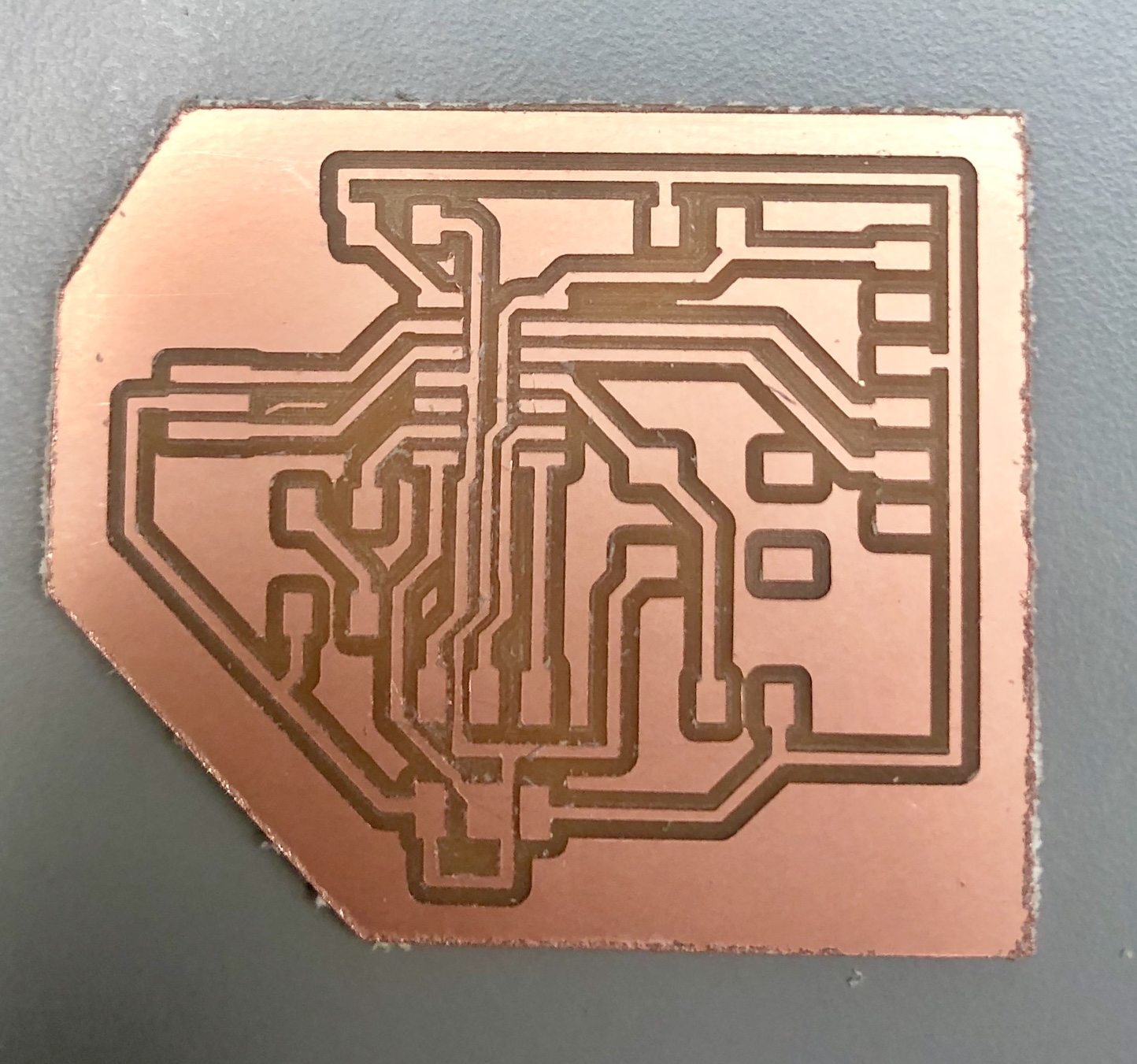
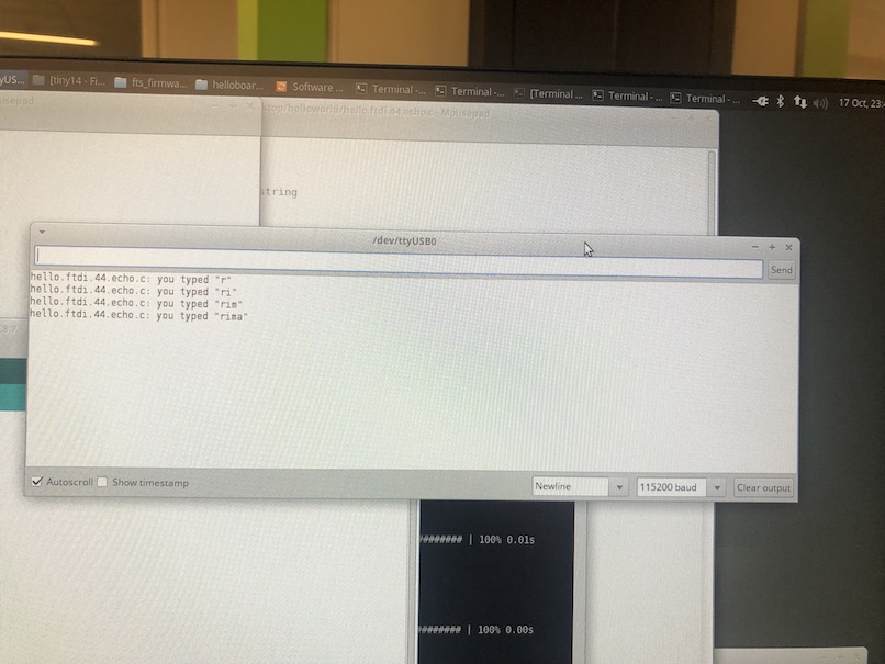
To program my board, I uploaded Neils makefile code from the website, using the programmer that I made from week 2. After uploading the code, my board worked which meaned I designed it properly! The board echoed my name when I went to test it.