Electronics Design
Now that we've got some good practice milling and soldering our PCBs from last week, it's time to learn how to actually design our own circuits so that we can send them to Clank. There are various software packages you can use to do this, but two of the most popular are Eagle and KiCad. Zach and Anthony each gave some really good trainings on these. Because of a tiny bit of previous experience with KiCad, I decided to dive into it more this week.
The assignment for the week is to recreate one of the echo hello-world boards, add some components to it, check the design rules, then mill, solder, and test it. I chose to remake the ATtiny3216 board.
In order to get all of the proper components into KiCad, I downloaded the KiCad Fab library for all of the components' schematics and footprints. In KiCad, I made to sure add everything in the "fab.pretty" folder to the Schematics Library, and the "fab.lib" file to the Footprints Library. Now that we have those downloaded and integrated with KiCad, we can start redrawing the board.
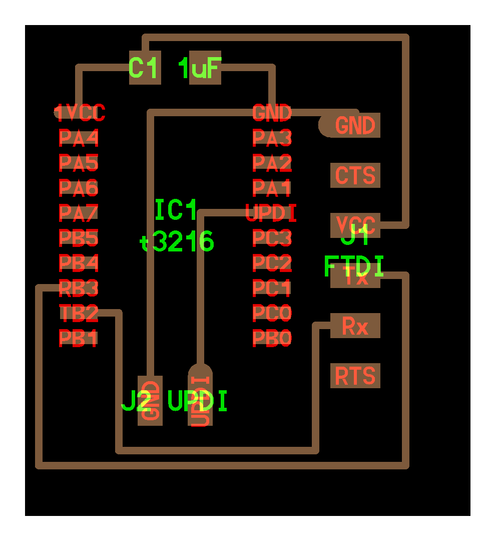
Here is the reference for the board I am recreating.
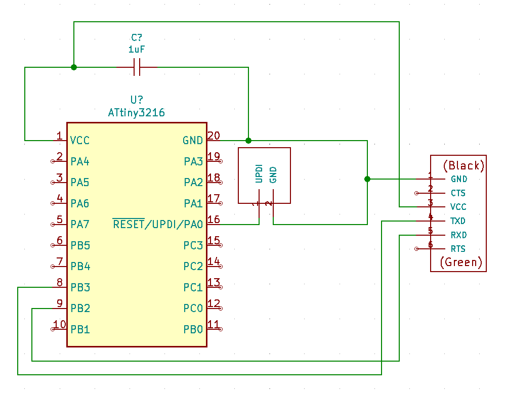
Here's my initial attempt at making all of the connections. It doesn't look perfect, but I am confident that all of the connections are wired up properly.
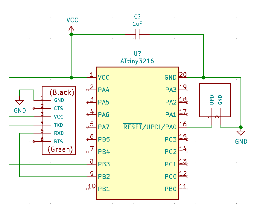
I moved some of the components around a bit to make a prettier schematic that is easier to read. Now, let's set the footprints for each of our components and generate the netlist so I can route the wires.
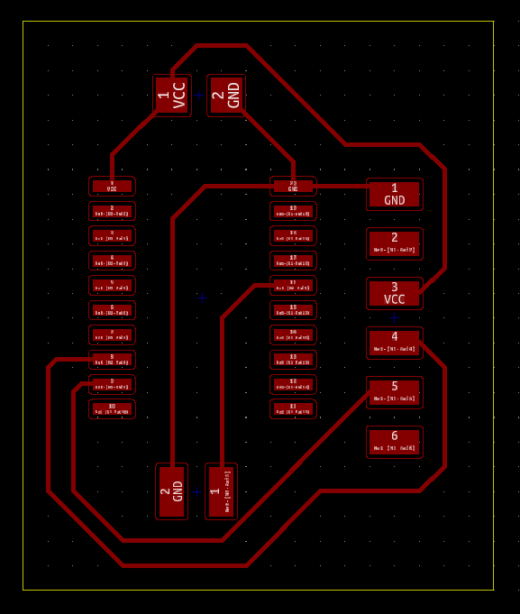
It was quite fun to untangle the rats nest and make things look really nice. This is the routing layout of that initial schematic. Let's compare it to the reference again.
Looks good to me! They both look pretty similar, except KiCad really likes 45° angles for the traces. Looks kind of cool, if you ask me. Now, it's time to go back and add some components. I could have added them from the beginning, but I wanted to first focus on recreating the circuit, then add stuff. Plus, it gives me experience going back and forth within the different stages of the design process in KiCad.
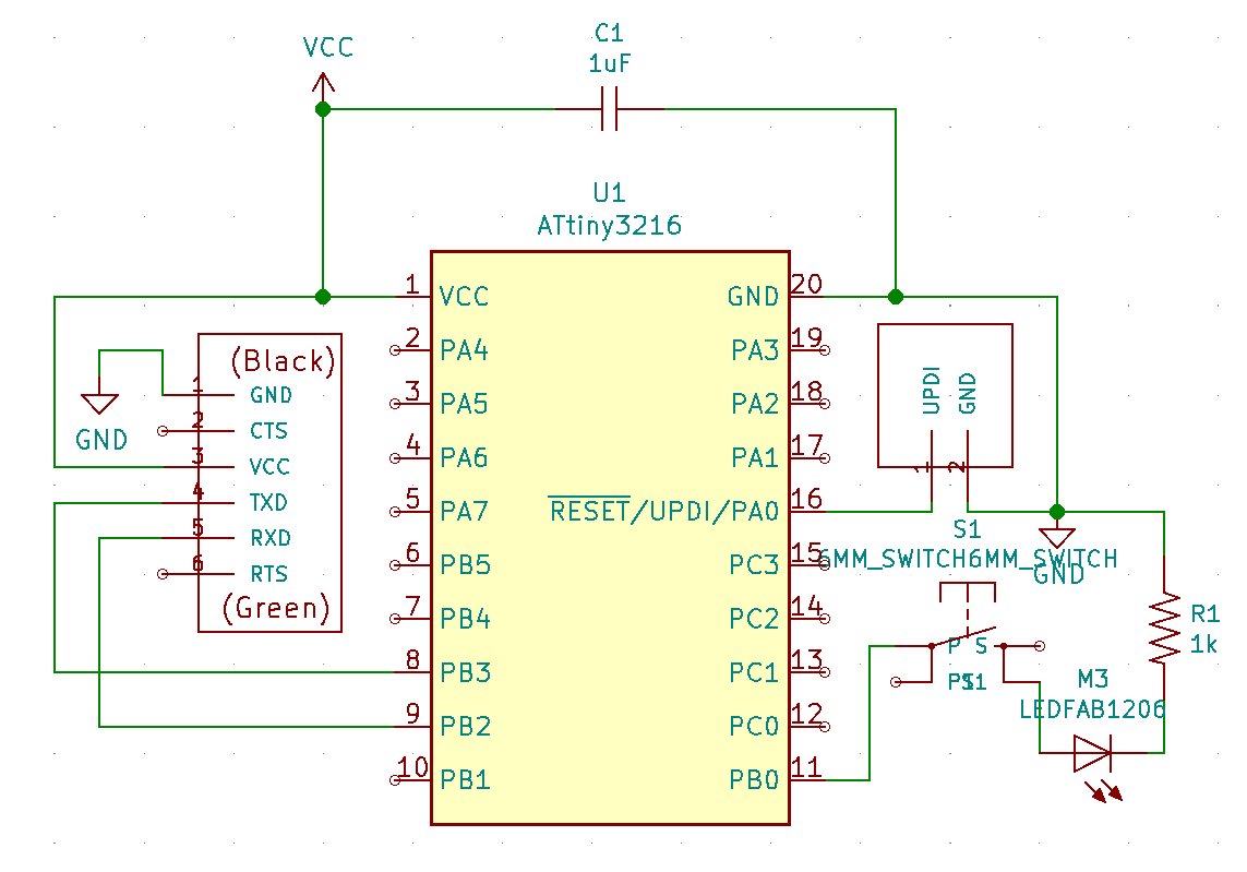
I decided to add a push-button switch and an LED to circuit, per the suggestion for the week's assignment. I also needed to add a current limiting resistor in there so the LED doesn't burn out. I connected these components in series to pin PB0.
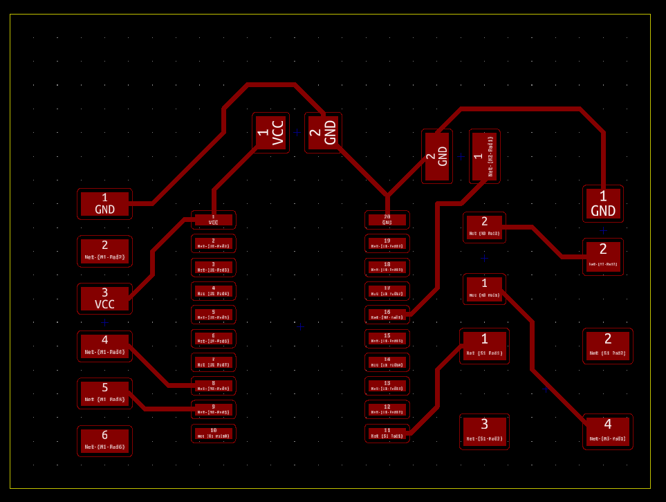
In order to arrange everything nicely, I decided to delete all of the existing routing traces so I could place everything where I wanted and then redraw everything. It turned out nicely, though, and I added the edge cut border. I then exported the two necessary layers as SVG files, and began preparing them for toolpathing. Zach's training (especially from 20:16 on in this video) was super helpful for this portion of the process, particularly in making sure the SVG had the correct export settings, then the next step of prepping it in Inkscape, which I will explain below.
It was quite the process to figure out how to get everything converted to the proper file types to work with mods correctly. There are quite a few options to choose from (go to the link, right-click, select "programs", select "open server program", then you have some options under the "G-code" and "Roland->mill" sections). I'm still learning how to use mods properly, and I'm sure I could figure out how to rearrange some things, but after a bunch of trial and error, what worked best for me was to import the SVG files into Inkscape, invert the colors, then export it as a PNG at 1000 dpi. This allowed me to use the "mill 2D PCB png" program in mods, which is what I heavily used last week. I still had some issues with this, but after fighting with the svg and png milling programs, I finally was able to generate some tool paths that worked for me. With all of this finally figured out, it was time to mill.
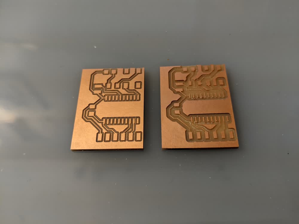
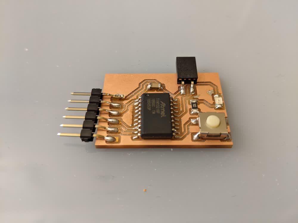
I decided to mill the board first with the 1/64" bit (on the right). Notable parameters to enter into mods are as follows: tool diameter = 0.0156 in, cut depth = 0.004 in, max depth = 0.004 in, offset number = 4, cut speed = 2.5 mm/s, plunge speed = 2.5 mm/s, jog speed = 10 mm/s, jog height = 2 mm/s, and spindle speed = 10000 RPM. If you look closely, you can see some burring going on around the pads for the ATtiny chip. There is also a trace between the button switch pad and resistor pad that got pulled up. They're technically still connected (I checked with the multimeter), but I wanted to try milling again with the 0.01" V-bit (on the left). The only parameters I changed for the V-bit was the tool diameter (0.01 in instead of 0.0156 in) and the spindle speed (11000 RPM instead of 10000 RPM). For both of the boards, I used the same parameters for the edge cuts using the 1/32", which are as follows: tool diameter = 0.0312 in, cut depth = 0.024 in, max depth = 0.072 in, offset number = 1, cut speed = 2.5 mm/s, plunge speed = 2.5 mm/s, jog speed = 10 mm/s, jog height = 2 mm/s, and spindle speed = 11000 RPM. You can see that the V-bit cut seems a lot smoother of a cut, but one thing that is particularly interesting is that the ATtiny pads seem to be bigger than on the 1/64" bit cut. I probably need to do some honing in of the parameters for the 1/64" to make some nicer cuts, but since I'm running short on time and am really satisfied with the V-bit cut, I'm going to continue on with that one. Time to solder.
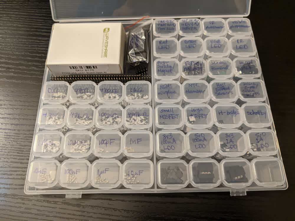
One thing that made this week much easier than last week was that I actually went through all of my electronic components and organized them. I know have a much better grasp on what I have, what they look like, etc. It seems pretty simple, but it has been so nice to know if I need to grab any other components from the shop or if I've got everything I need, and I can grab any of the components quickly without having to go through countless little labels and bags to find what I need. It took a while to do this, but was absolutely worth it.
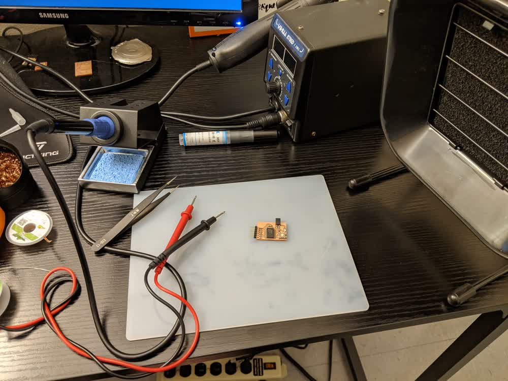
I struggled quite a bit with soldering last week as I have never soldered surface-mount components before, but Zach gave me some tips that helped tremendously (increase temperature from 350°C to 400°C, use the flat-end chisel tip, and use the flux pen), and I watched a YouTube video or two that taught me to put solder on one pad, then press the component on top of it while melting the solder that you already put down to lock it in place. Then you can go around and do the rest of the pins. It took some practice, but I finally got a result that I'm happy with.
I made a few mistakes, notably with the FTDI connector pins being slightly crooked and the top pin of that connector started to pull the copper pad up off of the substrate (I checked electrical connectivity with the multimeter, and it's still connected fine). Not all of my solder joints are absolutely beautiful, but I'm getting better and better with practice. One other thing to note is that I should have expanded the border of the edge cuts in some places so that the black part of the FTDI pins could rest on the board itself, and so that there was a bit more of on edge for the button switch and whatnot. Overall, though, it looks pretty good to me.
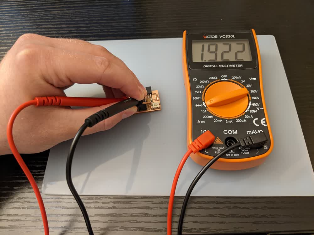
I'm pretty confident that I did this all properly, and as I have mentioned before, I did some testing with my multimeter to check that connections were solid. Everything seems good to go, and it is satisfying to hear the beep when I press the button, although it's very difficult to hold the probes in place and push the button at the same time... I also made sure to check that the LED was oriented properly using the same setting on the multimeter, and it is lighting up when the probes are in the right order.
I'm excited to get into designing my own custom boards for my final project, as well as learning how to program these boards. As I mentioned before, I've only really used pre-made boards that I soldered through-hole components to, so it's exciting to be able to design, mill, and stuff my own boards from scratch. I've also only ever really programmed Arduino right from the box, or someone had already set up the firmware and coding environment for whatever it was that I was programming, so it will be cool to get into the weeds of it all and understand it better.
Here are the files I generated for this week:
- week07_kicad.zip - All KiCad Files in a ZIP Folder
- week07-traces.svg - Traces SVG File
- week07-outline.svg - Outline SVG File