
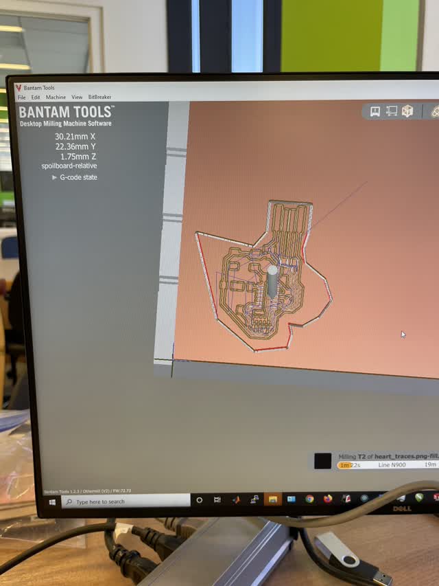
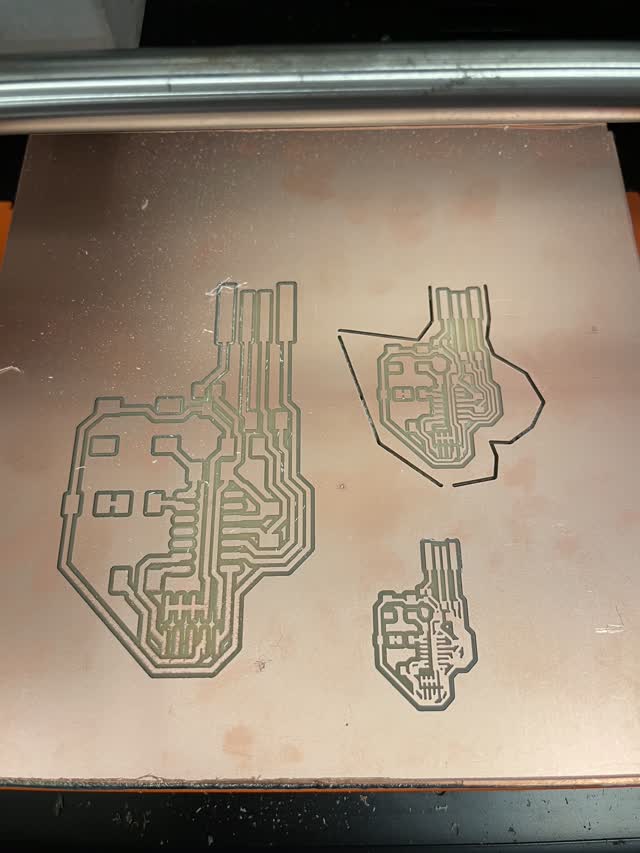
Milling a heart-shaped PCB board on the EECS MIT shop OtherMill machine.

For this week, I started by picking which PCB board to use and to modify with a button, and LED + resistor. In the end, after going to office hours and talking with classmates, I decided upon the ATSAMD21E board because I will be able to more easily use it for my future project (it has lots of available pins). Below is a comparison of the different boards I was deciding between:
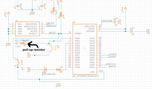
Now that I had picked my board, the ATSAMD21E echo, I proceeded to redesign this board in Eagle. I attempted to use KiCad but the libraries were not importing on my Mac (nor on another classmate's Mac laptop, either). The libraries seemed to load on Eagle in Fusion so I chose to proceed with that option.
This is the link to the library:
https://gitlab.fabcloud.org/pub/libraries/electronics/eagle
Make sure to watch to video here, in order to add the library completely!!
http://mtm.cba.mit.edu/2021/2021-10_htmaa-demo/
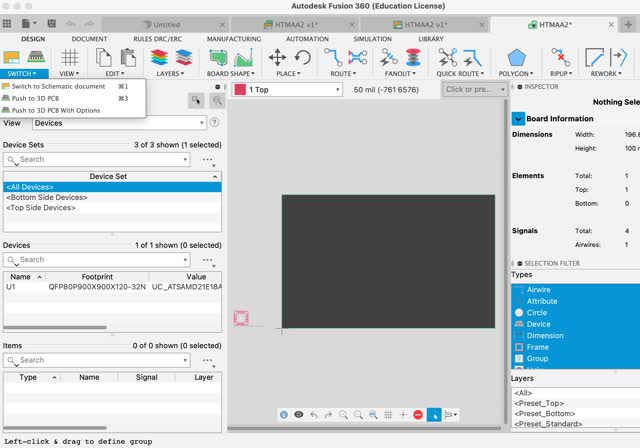
At first I had some struggles. One of the tabs randomly disappeared. But I figured out how to get it back by clicking on the Switch button In the upper left-hand corner.
I then had difficulty moving my PCB component in the PCB document view (with dark gray background).
Note that you can type in grid mm 0.1 to change the grid size, for example.
To move the PCB components:
1.In the command line, type in move and then press Enter
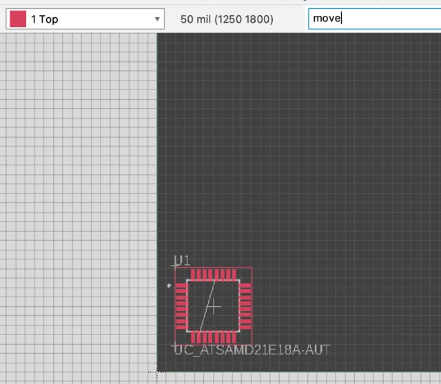
2. Use the cursor Just left the very CENTER of the component; if you select the edges it will not move! (at the center cross)

This should work for both the PCB document (gray background) and the schematic document (white background) view. You can switch between these layouts by clicking on the upper tabs at the very top of the winodw or usingthe upper right "switch" icon under the Design menu tab.
To rotate a PCB component: Right-click on the component and then select Rotate. OR, while adding a component before clicking to set its position, right click to rotate the component multiple times before left clicking to place it.
To move several components/wires at once:
To delete a wire or component: Type delete into the command line and then click on the component or wire to delete it.
I found an issue where I try to typemove into the command line but it gives a beep noise and doesn't work. To fix this, I saved my files, restarted Fusion 360 and re-opened my files. Then it could move components properly.
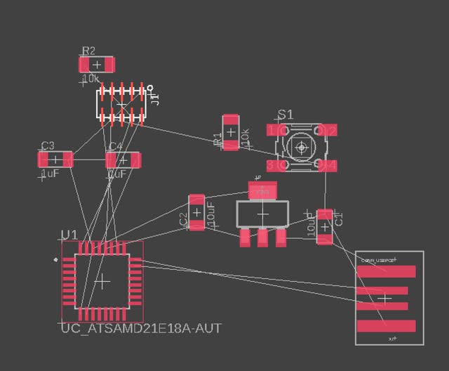
After adding the components in the white grid schematic, I was left with a tangle of componnets in the grey PCB document view. Yikes!
Next, while in the gray PCB board tab view, I typed in drc into thecommand line to open the settings for Eagle pcb design rules. I loaded fab2.dru from the Eagle library to set the design rules so that the traces & spacing would be large enough to be milled (e.g. with the 1/64" mill in the architecture shop). I changed from 16 milto 17 mil just to make things a little bit bigger, as the tutorial did (in the Clearance tab) and changed the minimum drill in the Sizes Tab to 0.8mm instead of 32 mil, again, just to make it a little bit bigger. Then I clicked Apply and Check.
https://gitlab.fabcloud.org/pub/libraries/electronics (fab2.dru location)
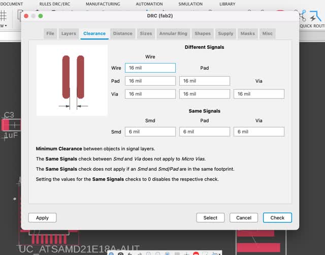 (Note: change 16 mil to 17 mil)
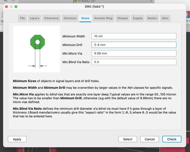
(Choose 0.8mm since it is just slightly larger than the width of an 1/32" end mill which is what we use to mill/cut into our board for the outline and vias.)
The error list mentioned Airwires, which means we have to draw the actual traces. To do so, I typed in route into the command line, and clicked on a pad and then clicked to set trace location anchors and then pressed on the other pad to connect it. The ripup command allows me to remove the routed lines that I had created. You can change trace thickness in the Route popup munu.
Next, upon realizing some of the lines cross & cannot be routed easily, I added a 0k resistor to jump over the crossing lines.


To get a more clean routing diagram: type in display -tvalues and display -tnames into the command line.
After going to office hours all day again over the long weekend, I learned how to add the resistor + LED and the button. I added a pullup resistor to the button so that it will read both on and off (rather than on/off and then stay reading at off due to the low voltage of GND taking over the signal).
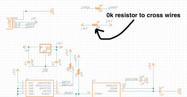
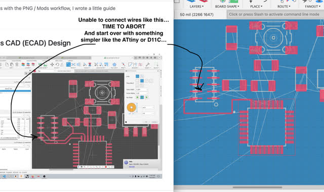
Unfortunately, I then got very stuck trying to route over crossing wires. I spent all day on this (LITERALLY) - and adding 0k Resistors wasn't working :(

I totally ran out of time and could not mill my board :( :( :(
Then I started getting syncing errors / ERC errors that the TA's couldn't fix in office hours Tues morning.
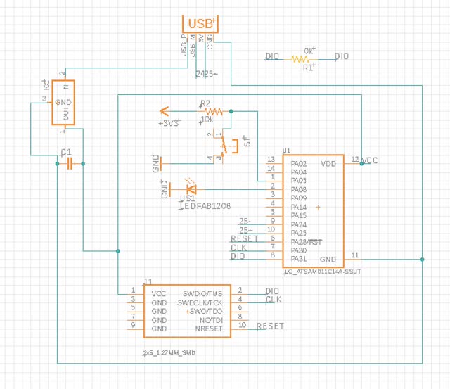
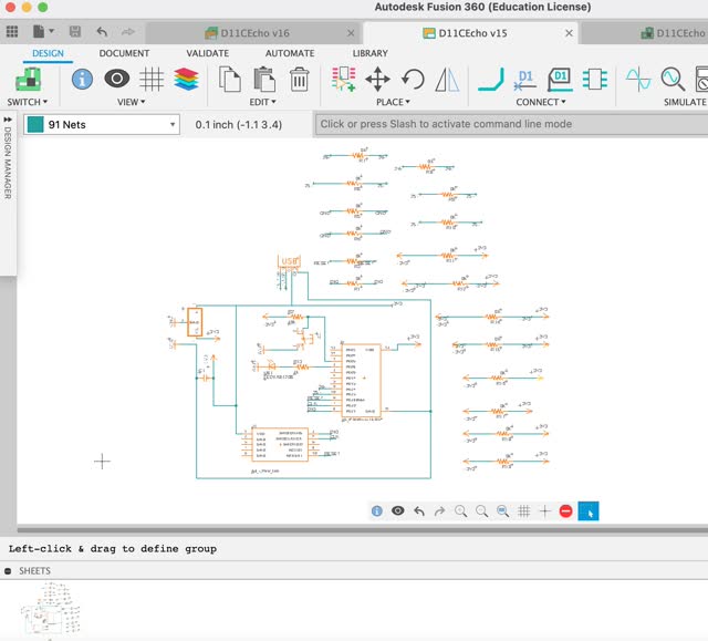
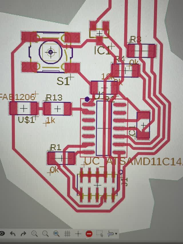
So I started all over again... re-starting from scratch with the Eagle tutorial, following literally step-by-ste, and making via's this time (that go through the board). I made a new schematic for D11C echo with a button & LED.
But once I again, I couldn't route it :( :(:( :,(
How to delete blue polygon?
In the grey layout, click right on the OUTLINE of the polymer (NOT the center). Then to draw the outline, click on the Board button.
How to close the blue polygon? Zoom in really far and click at the original spot you started the polygon at. Name the polygon as GND.
How to add a via on Mac (cannot middle click)? Type via into the command line and place it on top of the end of a trace.
You can use the name command in the command line to name via's as GND if you want.
How to hide the blue? NO IDEA...
display -tvalues & display -tnames to clear up the view
How to route wires properly? NO IDEA - it's not working the way the tutorial's wires are routing....
ABORT ABORT....
Time to move to the ATSAMD11C echo board with 10 pins:
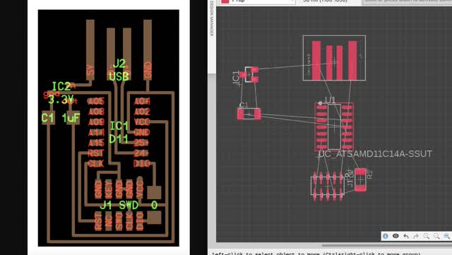
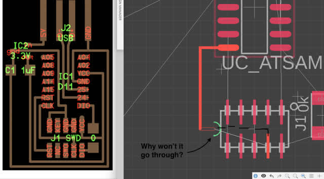
But I got stuck again for the same reason - unable to route wires through a component area... a little yellow circle kept showing up...

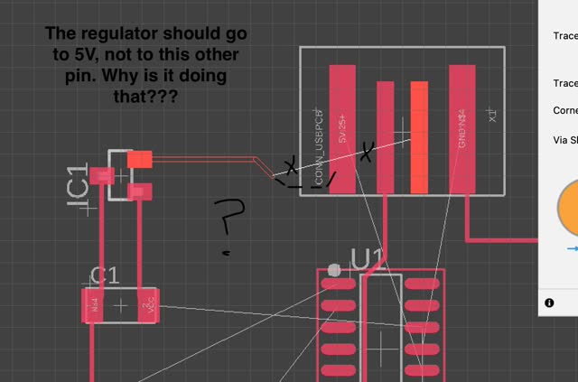
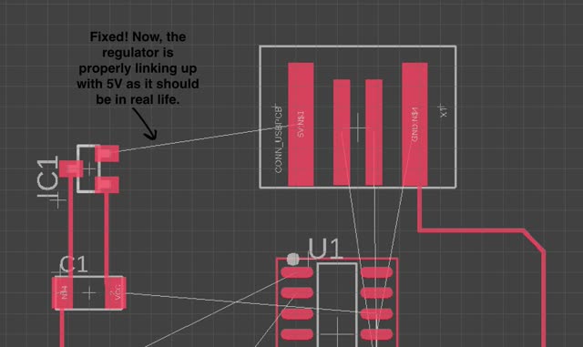
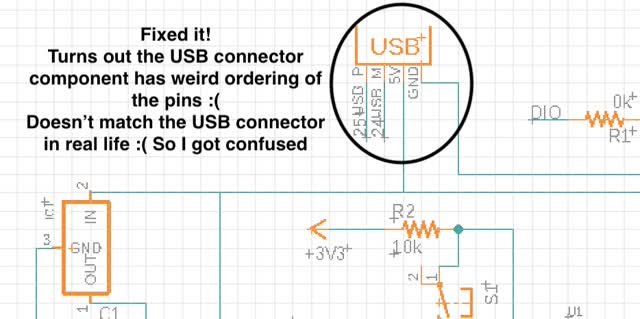
I was having major issues, also, with the white wires going to the wrong connection spots. But I figured out how to fix it, yay!

Here it is after I figured out what went wrong and how to fix it:
But now I am stuck again...
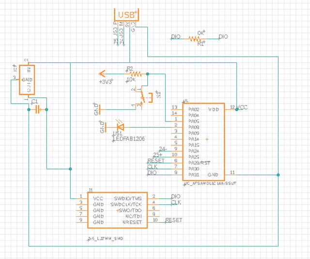
But my schematic looks right...
.... but when I finally got in to CBA evening office hours, the TA was super busy and I couldn't ask my questions.... :,(
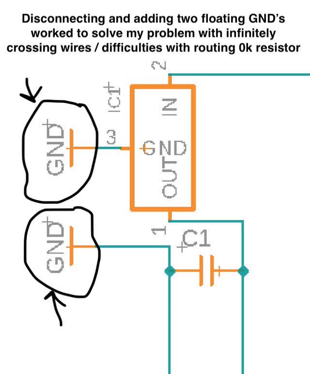
To fix the crossing wires issue when making 0K resistors, I found I needed to add more separate floating GND's in the schematic, which then fixed the issue.
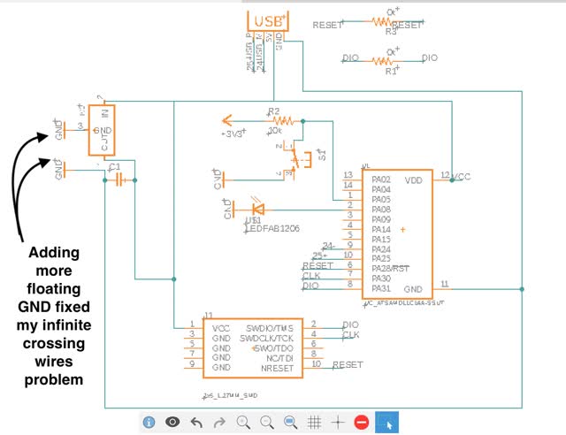
Then I did the same with +3V3 connections, making floating +3V3's instead of connected wires. That fixed the issues!!! Allowed me to add the 0k resistors without problems! :) :) :,) I also found that I forgot to add a resistor for the LED, so I added that in too, along with countless 0k resistors.
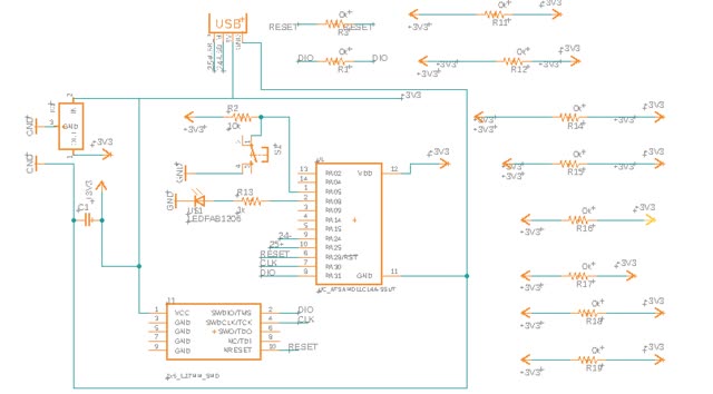
What a mess... but I finally learned how to route it! Yayyyy!!!
I planned to go in to the shop later to mill my board...
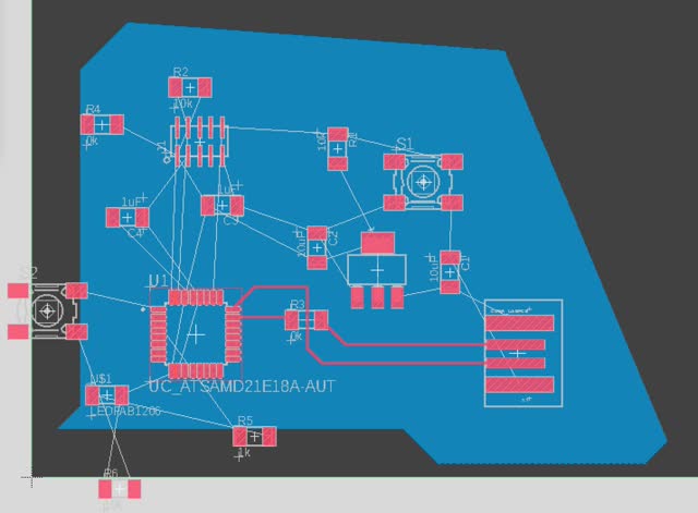
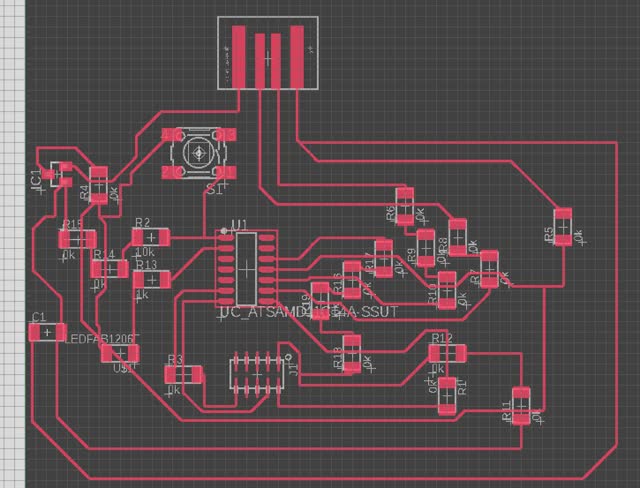
The next week, I met with the TA's to properly route my board.
Here were the tips from the TA on how to route better & faster:
I used a large DPI but the board came out way too big, like it was tripled in size. As you can see, the button is way too smallto be soldered properly onto the traces of this board that I milled!

So... to fix this, I calculated to change the DPI so that the resulting inches size would be small enough:
0.25in= button size
0.71875in = current size of board
So…
currently 3.472in long
Needs to be 3.472in *(0.25/0.71875) = 3.472in*0.34782609 = 1.207 in long instead.
So...I then tried changing DPI in mods until I got 1.207 in length (this ended up being 2876 DPI).

It seemed to work! The board was indeed scaled smaller. However, it appeared to be TOO small!
So then I tried 2000 DPI. But the outline at 2000 DPI showed up only half there - very weird! So then I tried to use 1800 DPI to make it slightly bigger DPI for the outline. But then it milled over the lines bady :,(


Maybe I will go back and try again everything at 1900 DPI... or get help from a TA. The person in the shop on this day was unable to answer my questions or help me with this scaling problem / outline problem.
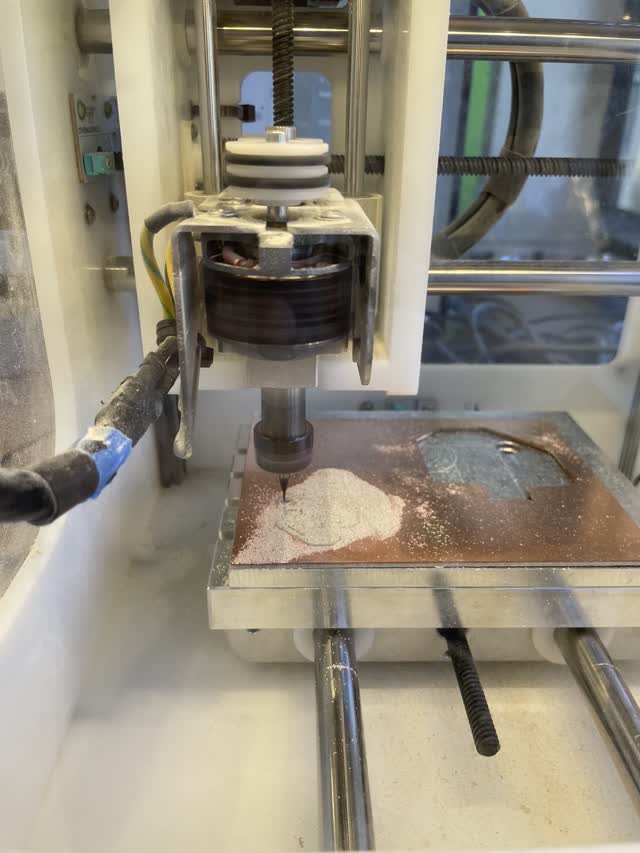
So then I went to the EECS shop (EDA) in 38-501. Carson (another student) kindly helped me get set up on the OtherMill and Mods in their shop (which worked quite differently compared to the Roland in the architecture shop!
Some differences:
I entered 2000 DPI in mods and Carson helped me use Bantam Tools software to do the rest. It came out okay!! (NO idea why!!??!!!)

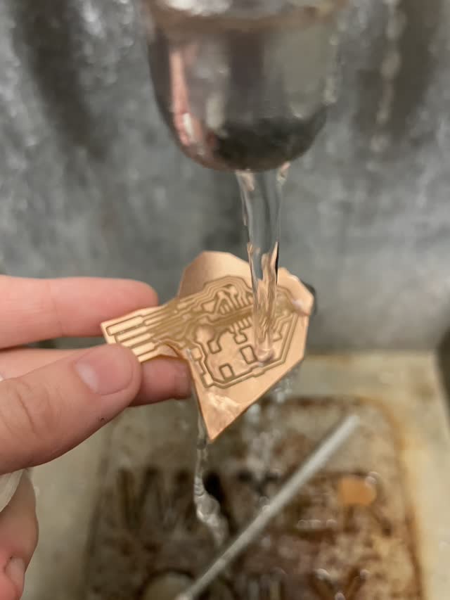
Next I cleaned my PCB board with Gojo orange soap 0955, which took away the debris to be ready for soldering! (The soap is abrasive, and works great for PCB boards. This soap is located near/behind the WaterJet equipment in the left hand shop of the architecture shop at MIT, near the back right of the room.

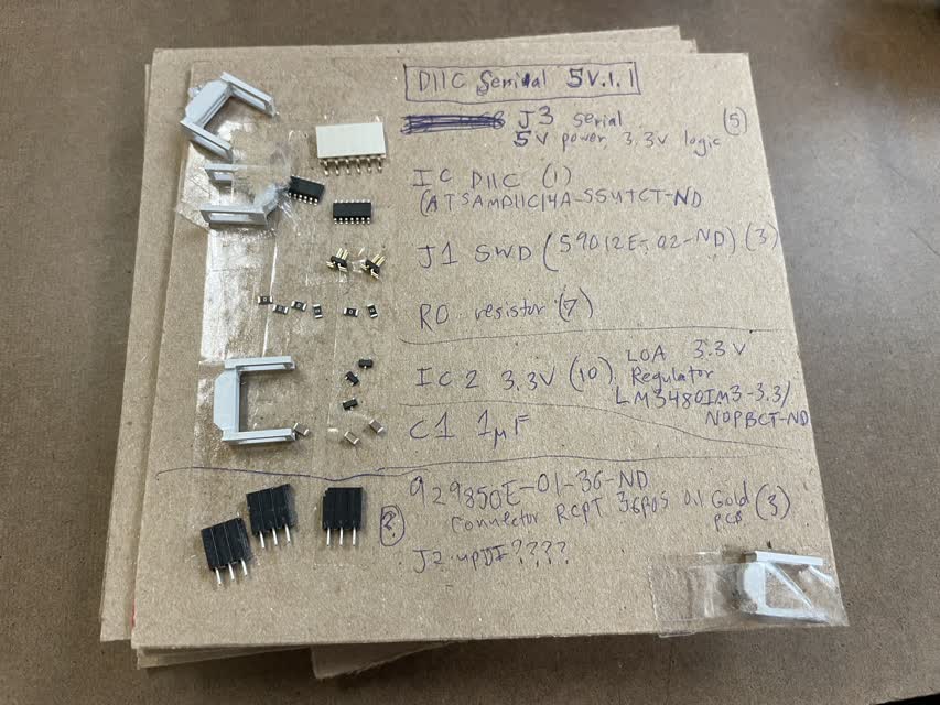
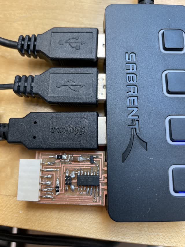
Next, I finished soldering (stuffing the PCB board)! Note that the numbers in parenthesis below represent the drawer set in which the PCB component is located within the MIT Architecture Shop (from left to right, up to down).
The students in the EECS shop also showed me their hot air gun, which is super useful for soldering on small components such as the microcontroller that has so many pins to solder!
Soldering was quite a fail, since I soldered the microcontroller backwards! The little dot on the microcontroller component needs to align with the purple dot in the schematic on the left!
So, I decided to re-mill and re-solder the board yet again... at 200 DPI, on the Roland in the archshop. I exported the PNG files to GIMP, added a size 70 x 70 black border, and exported the files again, except with 0 compression level.
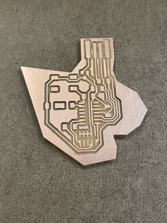
YAY! FINALLY, a good milled board!!! For extra caution, I milled two of them just in case!
(photo here of 2 of the boards)
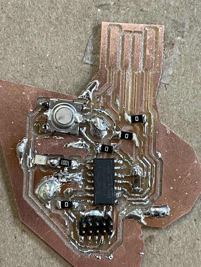
Then I soldered on the components. This time, I put the button and the microcontroller on in the right direction.
(Photo here of soldered board with annotations showing that microcontroller & button are in the right direction, and next to it insert photo of the schematic from Eagle with similar annotations showing the same with the dot / directionality.)
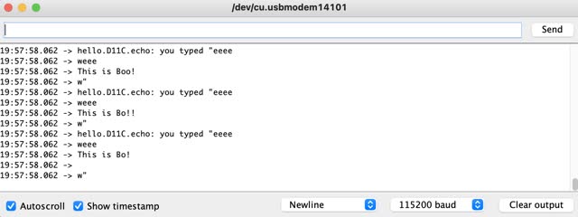
In future weeks I finally completed the board, bootloaded it, and tested an echo program:
(program is from echo.ino link for SAMD11C on the embedded programming week page on the cba course website)
http://academy.cba.mit.edu/classes/embedded_programming/D11C/hello.D11C.echo.ino

Hooray! Successful echo!
Here are the steps to add an extra border to GIMP to ensure part of your online doesn't get cut off during milling (in my case, it got cut off!):
1) Open GIMP desktop application
2) File > Open, and then open your original PNG files (traces file & outline file) that were outputted from Eagle or KiCad. Open each one of the files one-at-a-time (File > Open each time) so that they appear in GIMP on separate tabs at the top.
3) For each file, add a black border. First, go to Filters > Decor > Add Border
4) Type in 70 for x size and 70 for y size of the border
5) Click on the border color rectangle and choose 0, 0, 0 RGB to set the color to black.
6) For Delta Value on Color, select 0
7) Click OK. A border should appear equally all around the image.
8) File > Export As and then choose the file you want to export to (e.g. Downloads)
9) When exporting, make sure to set the Compression slider to zero!!!! (To 0)
10) All done! Now, just load the PNG to mods in the architecture shop for the Roland mill!
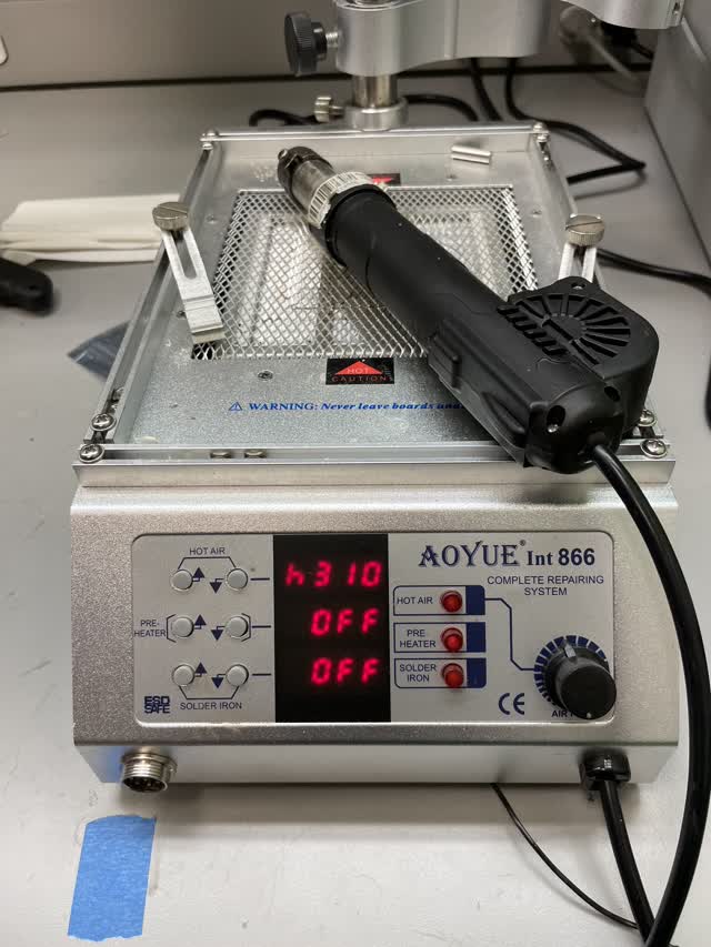
How to use the EECS MIT Shop Hot Air Gun For Soldering A Microcontroller Onto A PCB Board:
1) Solder wire onto the traces alone
2) Turn on hot air gun (on button on the back) and plug it in
3) Press Hot Air button
4) Turn up an down arrows for hot air; adjust to around 275 if going slow, and 310 if going fast for the time you spend applying the hot air
5) apply the hot air gun while using tweezers to position the microcontroller pins onto the traces of the board that have solder on them, which should be melting because of the hot air gun now!
6) Go back with normal solder iron setup if needed, to fix any areas that need to be fixed
Testing The Board:
To test the board with a multimeter, you can place the red and black leads onto the copper on the board and use either the sound setting or the voltage setting to test.

Sound setting: Board doesn't need to be plugged in to USB. Switch the multimeter dial to the sound/ohm setting. You can check whether your soldering has been done correctly by connecting the leads to different places on the board and if it beeps, then it's connected properly.
Voltage setting: Plug in the board to USB. Switch the multimeter dial to the Voltage setting. Then, you can do a couple of different tests:
Note that if the voltage reads as negative, then the flow is going from the black lead to the red lead, rather than the red lead to the black lead.


Learnings & More Advanced Applications:
I ran out of time but if I wanted to try additional test equipment, I could have tried the oscilloscope which can measure the actual signals coming through the wires (1's and 0's, for example). TA Jake showed us a quick demo of the oscilloscope.
An oscilloscope shows a graph of Voltage vs Time. You can change the voltage and time intervals if needed, to zoom in our out on the signal. On a portable oscilloscope, you can press a button to stop and start the signal, press another button to change the milliseconds on the x-axis (milliseconds per "division"). Triggering is what causes the waveform to appear at the same spot at the same time (starting a trace based on a falling vs rising edge of voltage). To measure the duration (width on the x-axis) of a bit, increase the time x-axis to zoom in. Put the cursors on either side of the pulse, and read off the x-axis width of the curve. To find one bit, zoom in to find the smallest (smallest width) curve and measure the x-axis distance for that curve.
In general, if you are using a multimeter and find that the signal is not stable at a particular value, or is an unexpected value, it can then be helpful to move onto an oscilloscope to check the individual bits.
Duty cycle tells you the % of time a cycle is high vs total signal, so for a servo motor it can tell you what position you're trying to send a motor to.
Learnings:
speed & cut rate...
Other Miscellaneous Notes:
NOTE: See video from last year on multimeters, to write this up!!
Components
Button: Usually, one nedof a button is hooked up to round and the other end is hooked up to an input pin of the microcontroller. When you press it, the pin gets shorted to Ground.
LED:
Resistor:
ATTiny412 in the electronics design page (makethat board)
UPDI is used for ATTiny in-system development
Hello Serial UPDI (serial to UPDI)
1)
hello.D11C serial.5V.1.1 is the programmer (in embedded programming)
2)
helloserial-UPDI.3 communicates with the Attiny (in embedded programming)
3)
Attiny board (ATtiny412) is in the electroncis design CBA website page
http://academy.cba.mit.edu/classes/embedded_programming/index.html#echo
Add a button and an LED to the 10 pin D11C board
http://academy.cba.mit.edu/classes/embedded_programming/D11C/hello.D11C.echo.png
ATSAMD21E (CBA shop says so)
SolderingKester 1 lb weight solder, Sn63PB37, 2.2%/245, Use it at 650 F temperature with smallest solder iron.
ATTiny uses
UPDI for AVR chip (ATTiny)
JTAG for ARM chips (SanD11C, for example)
ATTIny: pyupdi (command terminal use python 3 pyupidi... yourhextfile is your file location. That flashes the proram to your chip
FTDI to Serial: serial is the 4 lines, FTDI is the blackor whtie adapeteron teh bottomof it.
Use pyupdi
Use the ATTiny's
D11C is in short supply.
Motor driver...
KiCad:
press a to add a microcontroller (search for attiny412, take the fab one
hit a, hit VCC, drop it in.
hit a, hit GND, and drop it in.
press w for wire (when hoverin over a pin spot). click elsewhere to then complete teh wire.
open circle means it isn't a connected wire.
hit a, find C, then add that. (capacitor)
Rx = receive, Tx =transmit
FTDI header (Conn_pinheader_4.5mm spacing ... FTDI_1x06...
Click e to edit a field
hover over a symbol, and press R to rotate it
Right click onpart > orietnation > mirror (to flip the part)... can also press X.
Hover over a pin, press W, and tehn press the ending pin.
Fab library > R for resistor
Hit E and then type in the value of the resistor (e.g. 4.99k)
double click a wire to drop it without an ending.
hover over something and then press delete
bug symbol = rules check but don't run it...
L button to create a a label
Hit c for copy
Click assign PCB Footprint schematic symbols button...
Left click and then right click to open soemthig in the Assign Footprints page
File > Board setup > Design Rules > Net classes > change track width to 0.5mm andclearance to 0.5mm. Hit ok.
Hit net button... Update PCB & Close...
Hit M to move something around
X to put a wire down
Export SVG file > print board edges > export in black & white... then open in InkScape and maek them into svg or PNG to bring to mods.
File> document properties > resize page to the content > units mm >top margin: 1mm (same for bottom & side)
layer: cu
click left,
click right. Layer.Move to copper.
Click plus int he right hand.
Add it
hide coper
rigth click movelayer
outline
select
fill and stroke
fill black
File main menu > path > combine points
save copy as plain svg
\
created with
Website Builder Software .