Group Assignment: Observe Operation of a Microcontroller Circuit Board
From week 2 we already learned how to test connections on a circuit board using a multimeter. This is obviously a great first step, but it can only go so far. To get a more detailed look at our board, particularly while it's functioning, we should use an oscilloscope. Anthony showed us how to do this with a d11c microcontroller. He explained how to select a channel, and how to set the horizontal scale (time block), and vertical scale (voltage block). He then showed us how to connect the two probes at different points on the circuit and observe the signal on the screen. For example, in the image below we see signal switching between high and low, and this represents the bits being sent down the USB connection (1 for high, 0 for low).


Individual Assignment: Custom Echo Board
Schematic and PCB Layout Design in Eagle
For this week we had to design our own echo hello-world board! There were multiple boards to choose from, but after reading the help page that my amazing TA Laura made for us, it really cleared things up in terms of how to program the various boards (depending on ARM or AVR) and what auxiliary boards are needed. Ultimately I decided to go with the 10 pin ATSAMD11C board because it has a USB connection and because it has the 10 pin connector, it can be programmed directly by an Atmel-Ice (loading the bootloader). From that point forward I can load programs directly onto my board from my own computer!
After deciding my base board, I set off on building the schematic and pcb layout. I used Eagle primarily because I'm already using Fusion 360 for my CAD modeling. I found Jake's tutorial to be super helpful for learning the different commands/keyboard shortcuts/best practices. Here is my schematic and pcb layout:
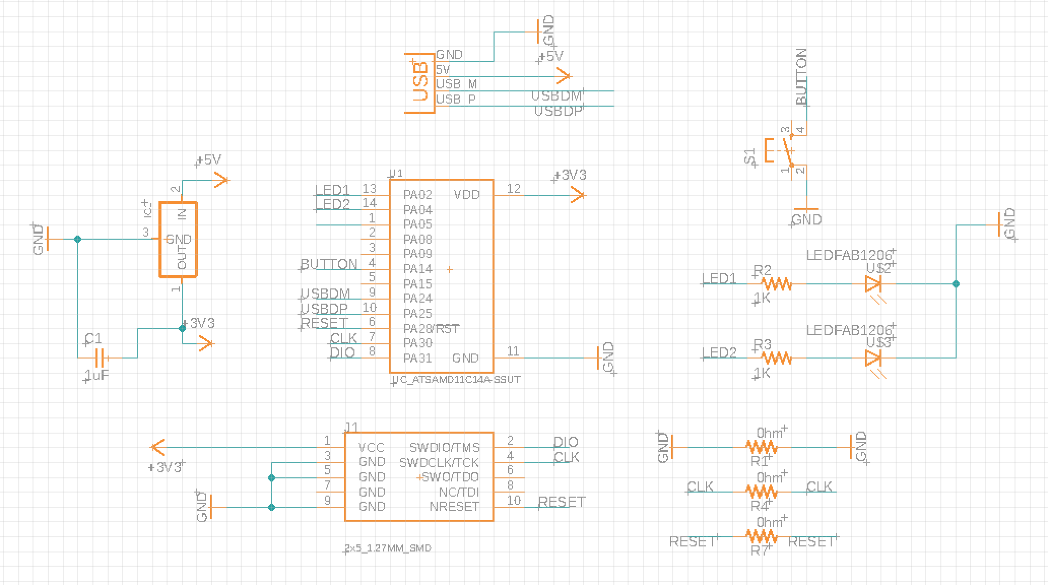
I imported the fab library of parts into Eagle to make sure I was selecting the components that were available to us in the shop. I'm pretty proud of how relatively clean (albeit simple) my schematic is. I used the 'label' feature heavily so that I could logically define connections rather than having to manually connect them - I highly recommend this. I added my two LED's to pin's A02 and A04, which are both analog pins. I connected my button to pin A14 which is a digital pin. I ended up needing three 0hm resistors to act as jumpers.

For my pcb layout, I started by loading the fab DRC rules so that I would make sure not to violate any of the design rules of my mill. It took me several (like 5 or 6) different iterations to nail down the layout (though I'm sure it can be done more compact and with fewer 0hm resistors). I actually quite enjoyed the tackling ratsnest problem. I approached it by starting with my most highly connect components (the d11c and 10 pin header), and worked my way outwards. I also made my ground and 3.3V power lines go around the boundary of the board since a lot of components will want to connect to them, and this made them more accessible. To make my soldering easier, I decided to use 0.5mm for my route width. Obviously this would increase the size of my board, but it was a tradeoff I was willing to make :) For the traces in between the d11c I reduced the width to 0.254mm so that I could fit multiple.
From here all that was left was to export my traces and outline (separately). I again followed the instructions that Jake provided in his tutorial. I exported both as PNGs with 1000 DPI. Here are the raw images when exported from Eagle:


For some reason, Eagle would add extra black space to the right side of my images (which is not problematic but still annoying), and it would place my traces/outline very close to the left edge. This turned out to be problematic because when I would load these into mods, mods would actually not detect the left edge of my outline! To fix this issue, I used GIMP to add a small border around both images (note that I had to add the border to both images because they needed both have the same (0,0) point). Here is what they looked like after adding the border:


Now that we have the PNGs, it's time to mill them!
Milling the PCB
Failure 1: Lol It's Huge!
Thankfully working with the Roland mill this time around was much easier. I remembered how to swap out the different end-mills (1/64 and 1/32), and how to correctly callibrate in mods (well, sorta). I got right to it and starting milling my custom PCB. I started with the traces, and then the outline, and here is my first attempt:

As you can see, it's HUGE! While it was milling I had a feeling something was off. Firstly, it was taking a really really long time to mill, and secondly, I was suspicous of the size of the USB connection. I was like "hmm...this seems too big, but maybe it's right? Eh let it finish." I included a normal size PCB for size comparison. At this point I had a minor panic attack and I frantically reached out to Laura and Jake for help. Laura was gracious enough to help me debug the problem, and she pointed out that my DPI was wrong. I had left the DPI at 1000 in mods (because that is what I set in Eagle). However, because I exported my images from a mac with retina display, I was actually suppossed double the DPI to 2000 in mods (apparently this is long standing Eagle bug). This solved my size issue, onto the second failure...
Failure 2: Different (0,0)'s
After correcting the DPI, I remilled my board, and here is the result:

I was relieved to see the size issue fixed, but as you can see my outline is slightly offset. This is obviously problematic because the right edge of my board is gone (my ground trace). Jake helped me realize that my traces PNG and outline PNG are slightly offset - I must have messed something up when adding the border in GIMP. I (carefully) went through the process of adding a border again, and I finally got my first success...
Success 1: A Little Chewed Up
After fixing the offset issue, I finally got my first successfully milled custom PCB board:


All the traces are there as they should be. The only minor issue is that the board appears a little chewed up, as you can tell by closeup. I suspect this is because of of the end-mill. Anthony later told me that completely fine board, just needs a little sanding. However, in the moment I was unsure so I decided to try a different 1/64 end-mill and try again:
Success 2: 4th Time's a Charm!
After swapping the end-mill, I finally got the result I was looking for! Unfortunately I was too excited in the moment and forgot to take a picture of it :) But, here is a photo of it stuffed with all the components:

Soldering this time was much easier! I think partly due to experience/confidence, and partly due to the larger footprint sizes. Weirdly, I found soldering the board to be the easiest part of the whole week. Lastly, here is the progression of my milled boards:

Programming the PCB
With my board soldered and ready to go, next step is to program it. Laura helped me out here. First she loaded my board with the bootloader using the Atmel-ICE. Once that worked, the next step was to load the echo program onto it, and that worked also!


Testing the PCB
Lastly, I wanted to test my PCB using the oscilloscope. I plugged in my board, and I wanted to make sure I could measure 3.3V when I connect from the output of my voltage regulator to my ground. As you can see, the oscilloscope reads 3.2639V, which is very close to 3.3V!


Files
Eagle Design FileBoard Traces (remember to set DPI 2000 in mods!)
Board Outline (remember to set DPI 2000 in mods!)