Final Project
Content
- 1. Introduction
- 2. Theoretical background
- 3. Fabubox
- 4. Spin coater
- 5. Hot plate
- 6. Organic solar cell manufacturing
- 7. Strain gauge manufacturing
1. Introduction
As the description of this class says,
How to make almost everyhting broke a huge part of that fear. I designed, milled and solder my firsrs PCBs .That helped me to understand components.
Machines that makes machines helped me to understand much more about sensors, what are we reading when we are sensing, how a physical device can generate signals to became a physical - digital device, the noise around it and how to deal with it.
PIT is helping me to understand what is going on inside the component by making a bigger emphasis on semiconductors.
- Can I design and manufacture a classic 101 PN junction device, a Solar Cell?
And with this questions comes more:
- Can I manufacture using FabLabs tools only? If yes, which other electronic devices could I manufacture in house? Could that be part of FabLabs 2.0?
Well, lots of people. As my project is more about understanding basic physics I am not providing anything new to the field. My friend
If talking exclusively around PN - junctions that transforms Solar radiation into electrical current, you will find more more information in the
First, a big layer of semiconductor theory reading that you can fing in the section
Second, Ive learn from Jan lots of Fab processes, asked him 1000 questions and built some of the components needed to replicate those manufacturing processes in house. You can find more information about those tools in the
Third , built the platform, we compared MIT Nano processes with our in house process and meassured thickness values with ellipsometry.
Forth, once validated our methods, I started spinning elements to manufacture semiconductor devices and other fun components using phothoresistors! We built as our first component strain gauges. Once we optimized the process, install all elements in the box and ensure its performance, we start spinning on glass ZnO and PV2000:PCMB on pre worked substrates. Later, using an Angstrom Vapor Deposition System we deposed 50 A of MoO2 and 1000 A of Ag. Once deposited, we encapsulated the solar cell and characterize it measuing the External Quantum Efficiency (EQE) and the I-V curve under the solar spectrum.
First theoretic questions that I will adress in the theory questions, then microfab questions. We need to callibrate our tools to make process which we needed to be very precise in thickness characterization and temperature controll. Then, organic solar cells vs silicon based solar cells. And then, what does all the characterization charts means.
We have been able to validate some process for what we seen as an accessible building platform for Fab in house without the need of a large clean room and all it consequences. We have been able to make a very efficient solar cell and a functional strain gauge. Many many things broke along the process. We couldnt do the vapor deposition inside of the box and we can not controll the resistance values of our strain gauges.
For the solar cell, we see that it behaves (almost!) as a perfect diod when submitted to current at no visible spectrum. We see that, when we hit with light, we start perfoming as a solar cell with an state of the art performance for an organic one. Then we show a functional strain gauge !
I learned a lot about semiconductors. I build tools that helps building solar cells and thin deposition processes.
2. Theoretical background
Most of the content for this chapter is taken from:
2.1 CRISTALINE STRUCTURE OF MATERIALS
A crystal is defined as substances whose properties reveal the presence of an ordered structure. For example, we can see an
Cristaline structures are atomic lattices arrangements composed by the repetition of one or more unit cells. That type of arrangements generates concepts as lattice spacing, crystallographic axes and lattice spacing.
The outer shell electrons are the responsible of atoms being arranged in a 3D geometrical order . They will also provide physical properties to the material. As an example, lets take the structure of Si as it helps to understan what is a P-type semiconductor and a N-type semiconductor.
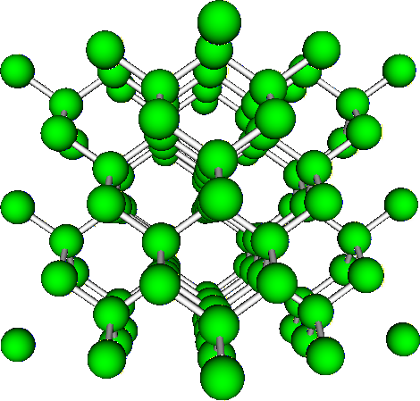
[Si cristal along the <110> direction, https://www.iue.tuwien.ac.at/phd/hoessinger/node26.html ]
2.2 ENERGY BANDS
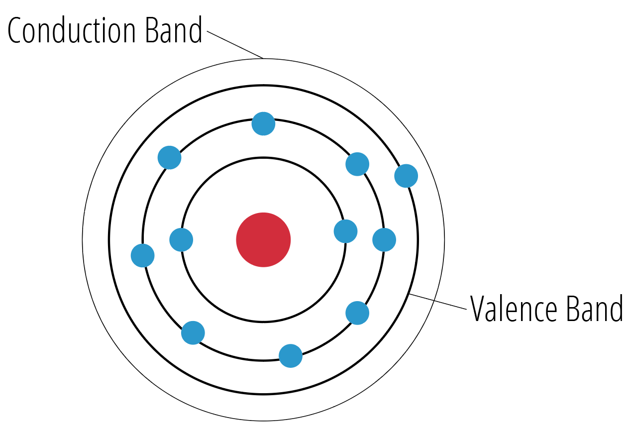
[atoms and bands]
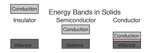
In an atom, the external shell or orbityn atoms is called the Valence band. Electrons in the valance band could. Insulator, semiconductors and conductors have different energy levels for an atom to jump from the valence band to the conduction band. The large the energy gap is, means that for examples, isulators electrons wont reach this energy at all at ordinary temperatures.
On the other hand, semiconductors and conductors, their band gap is small enough that thermal energy could make an electron jump to the conductive band.
[Energy levels]
2.3 DOPING AND P-N JUNCTIONS
With this known , take now Si, and lets see his strucrture. Si have 4 Valence electrons. In a cristaline structure, , a grid of silicon atoms will form covalence bonds along all its perimeters.
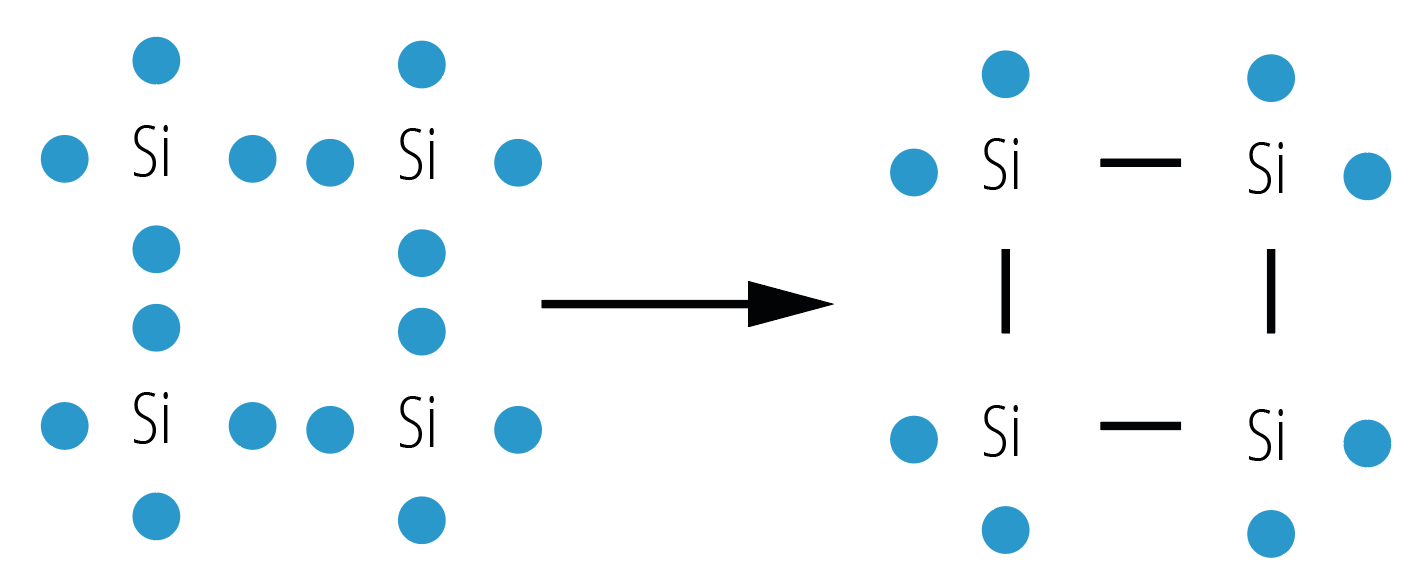
[Silicon Covalence Bonds]
So.. what happens if we add impurities to the Si structure doping it with phosporus? P have 5 electrons in the valence band! This electron now is able to jump from valence to conductive band and move freely through the crystal. We have increase conductivity of Si by adding an element with 5 electrons in the valence layer, chargint it negatively. This type of semiconductor is called N- type.
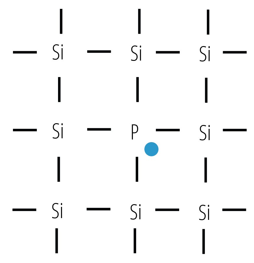
[Silicon with added P]
What if now, we add an element that has less electrons in the valence layer than Si as for example, Aluminum (has 3)
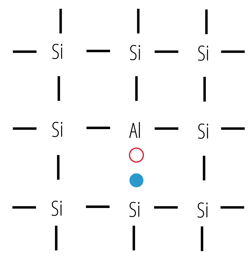
[Silicon with added Al]
We have a lack of an electron, also called Gap! That Si electron is now able to again move in the cystal structure, creating a P-type semiconductor. The charge carriers are holes .The movements of hole is the responsive of increasing conductivity of Si.
So now, what would happen if we are able to grow,
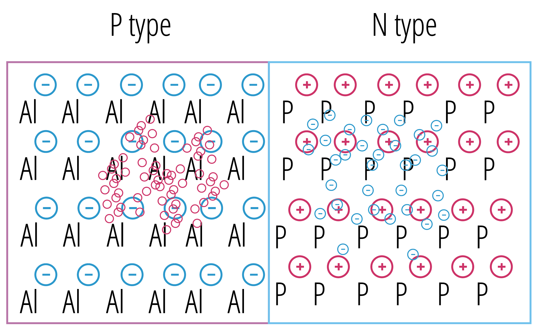
[P N Junction. Left a negative ion produced a bunch of holes, right, in the N side, a positive dope element produce free electrons. ]
At the left , holes created by the add of aluminum generate holes as majority charge carriers. At the right, A, a group 15 element, Al ions cant move but there are some free electons randomly moving around.
The single crystal created will at first, diffuse in the boundary . Holes and electrons will destroy each other in that region.
But that only happens in the junction area. Diffussion wont continue all the way down because the charges now are exposed!
When a N electron wants to travel to the P side it will be repelled by the negative ion (Al). Same for the holes. The exposed inmovile ions creates a barrier for diffusion. The more they diffuse, the more ions are exposed. Diffusion moves electrons, from N to P, so there is a Current flowing from P to N! Idiff
Now is when minority charges takes a big role.
[Minority charges moving]
This movement generate a current in the opposite direction called I drift (N to P). In the inner region, the chrged part of the semiconductor there is an Electric field! This field goes from N to P and minority charges are atracted by this drifting motion.
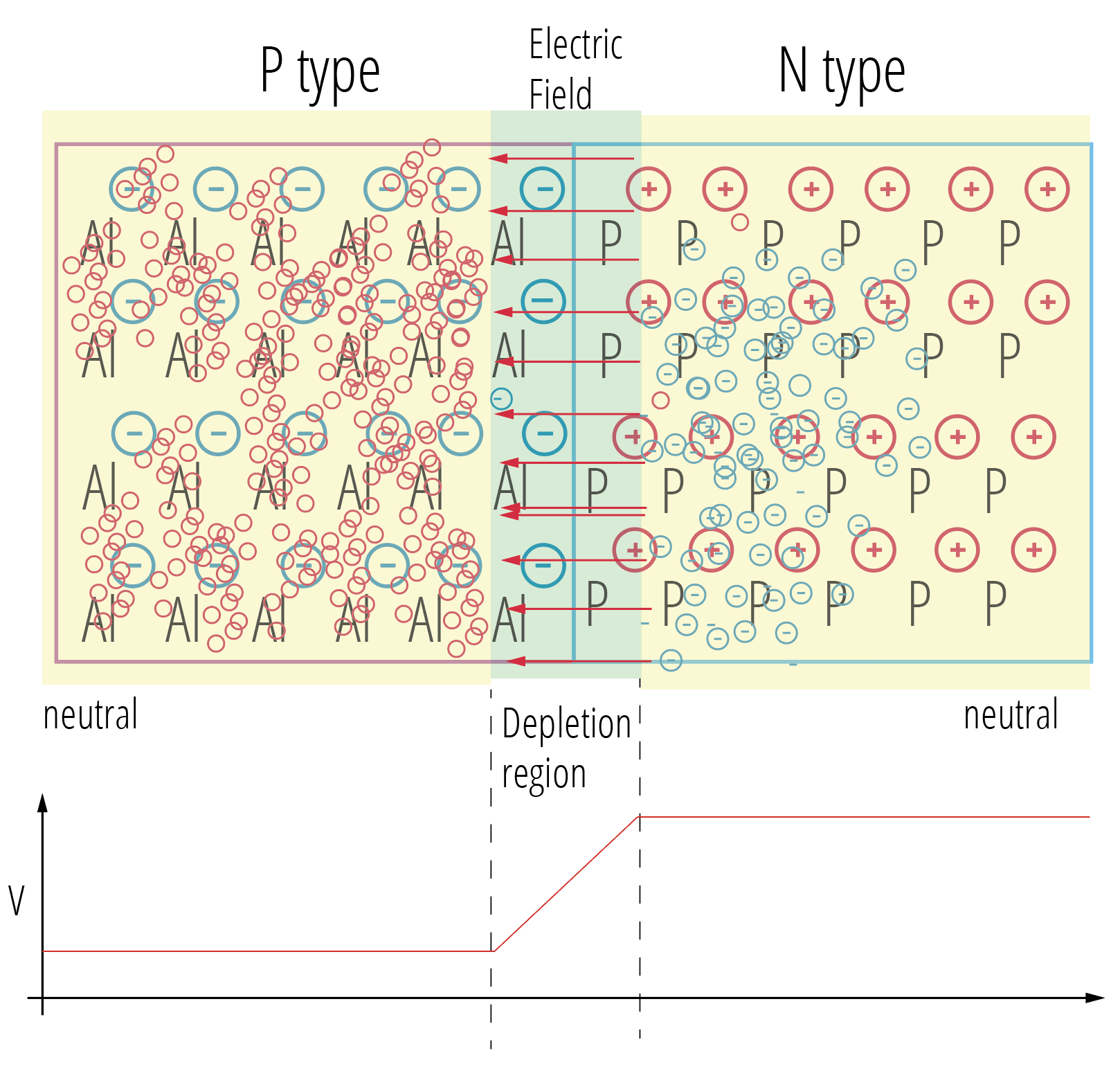
[We have an intrinsic voltage!]
2.6 SOLAR CELLS
In the depletion region,
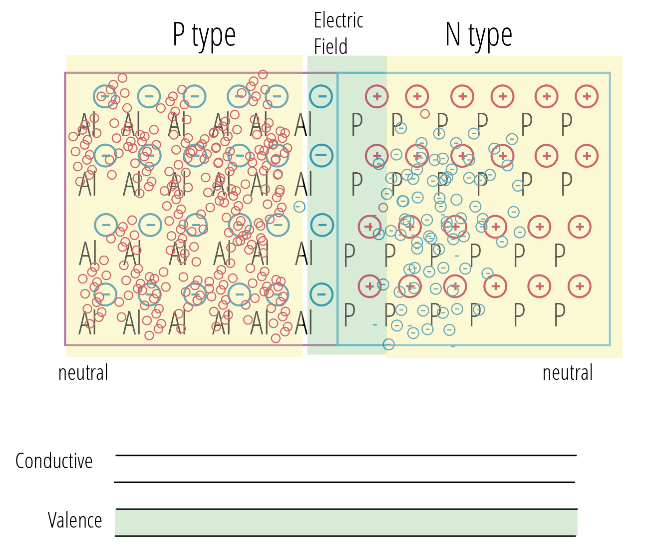
[Valence is full. ]
But, when a photon comes with sufficient energy that makes one of the elections jumps into the conductive band. When this happen in the depletion region things gets so interesting.
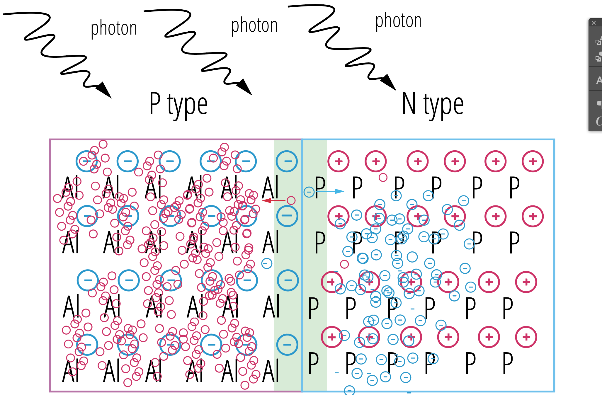
[Electron jumps to N, hole is created, they get atracted by its medium and cant recombine. That make a current flow. ]
Before they have a chance to recombine, they are swept across the material making a current to flow!!
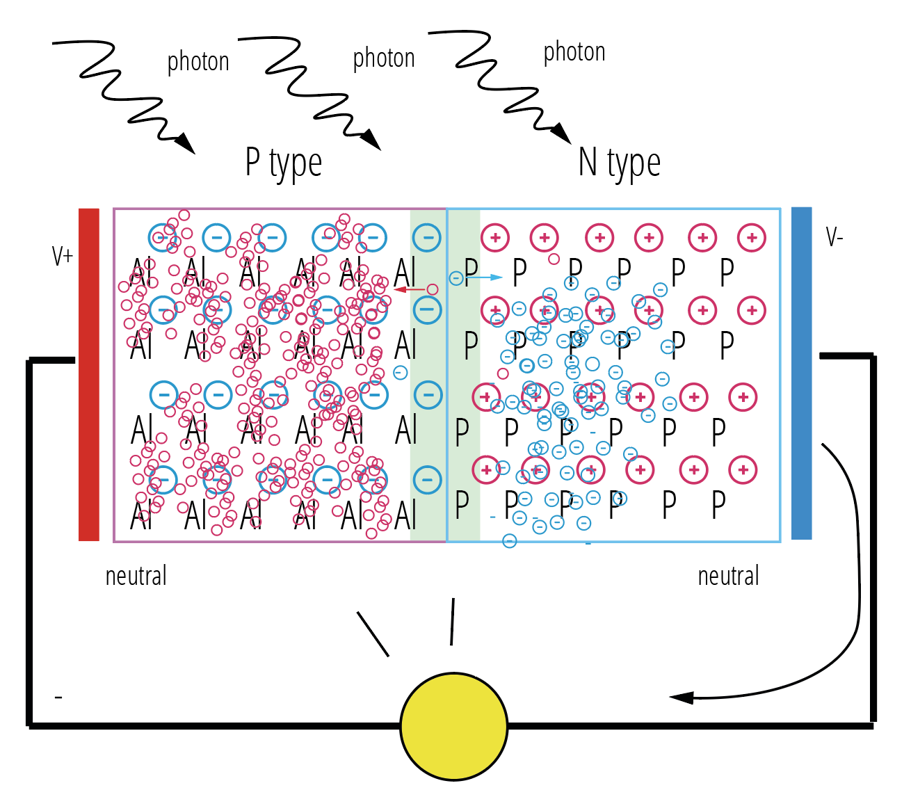
[If the sun still hiting, we will create a constant voltage that will flow a current when hooked up plates in the anod and cathood! ]
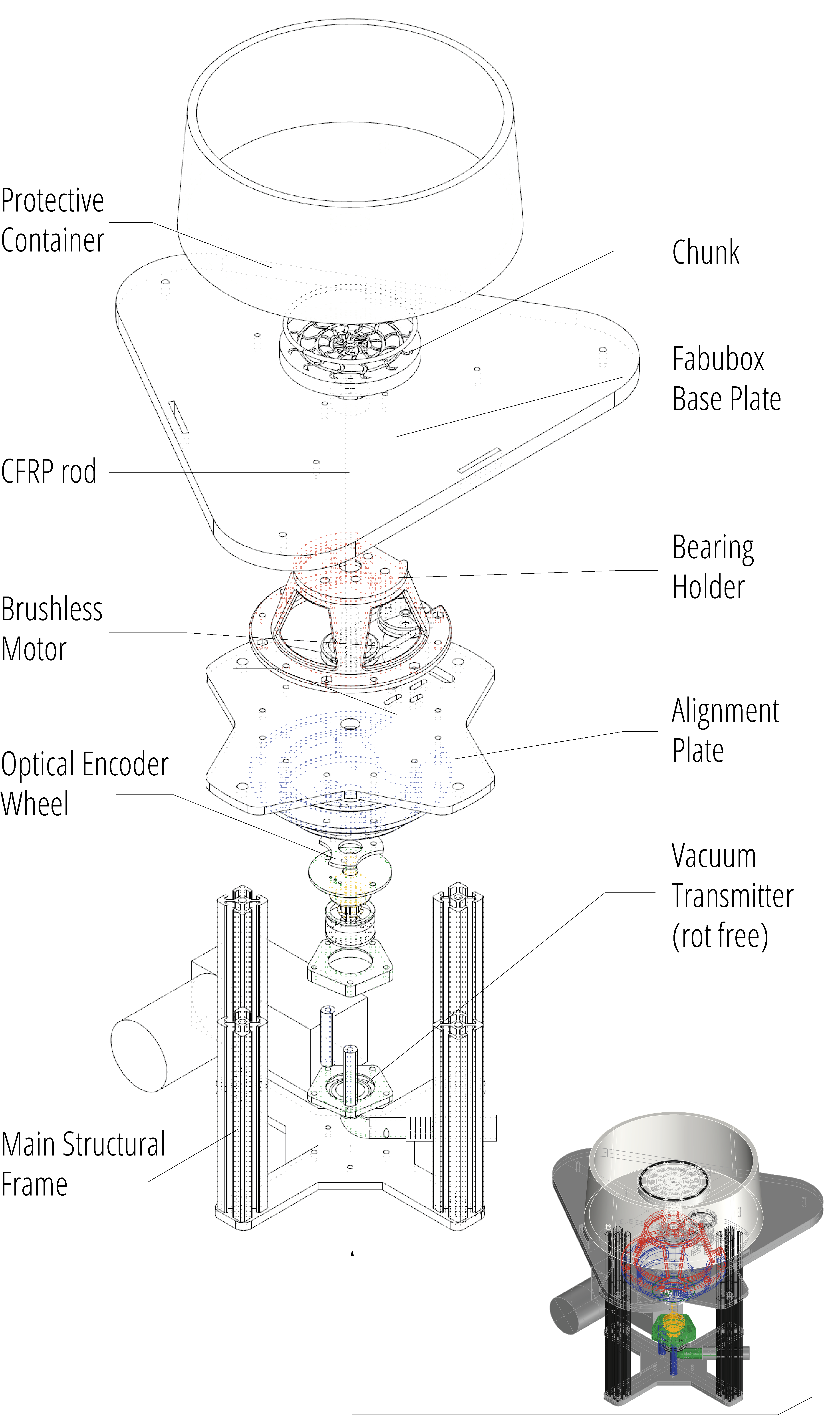
3. Fabubox
TBDocumented
4. Spin Coater
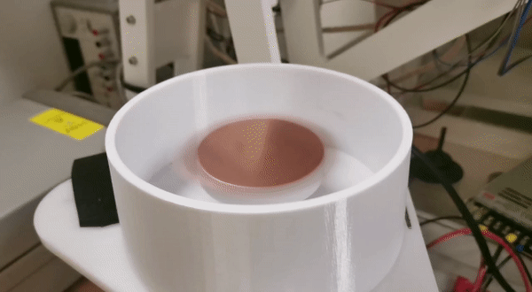
Spin Coating is a central part of all semiconductor industry, mems, sensor, integrated photonic, antennas. All that start with a spin coating process. It is a solid manufacturing method to fabricate thin films consistently controlling the thickness in the nano - micro order of magnitude.
Off the shelf spin coaters prices can be around $2k.This access cost can be dramatically dropped down if we design some parts and choose a smaller vacuum pump. We have found that there are ways to make a close loop Spin coater with all elements found in the Fab Lab shelves to be worth around $80.
Find here the spin coater done for this class:
[$80 Spin Coater]
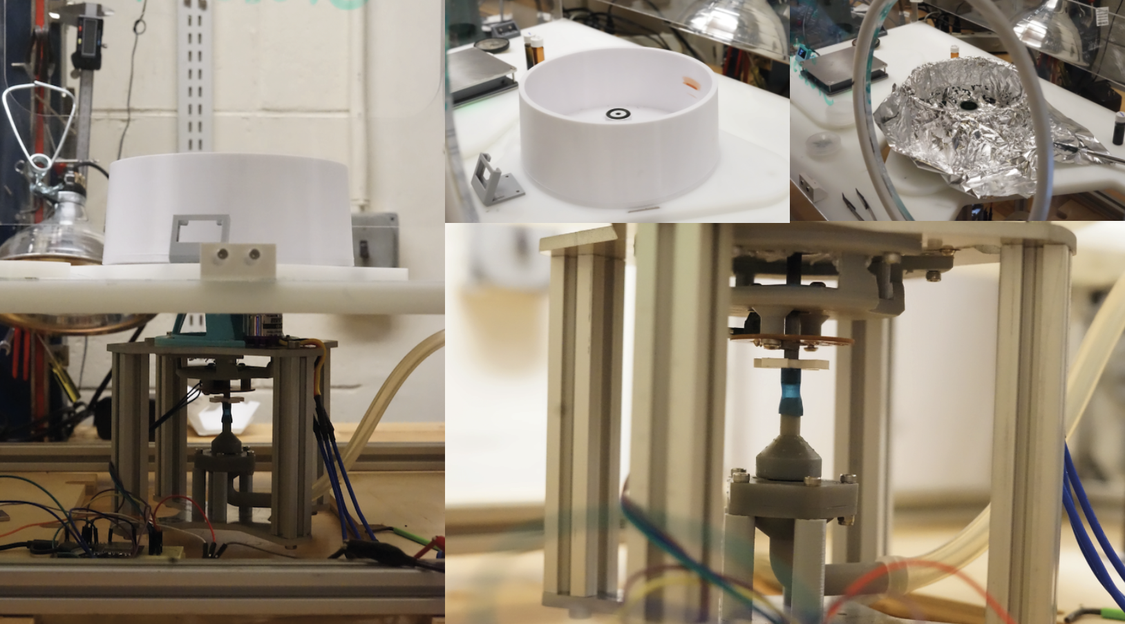
[Spin Coater doing its stuff well]
Something I am really happy about is the mechanism used to keep on transmitting vacuum while having a rotational degree of freedoom. Not only be free, but a device that can rotate up to 11k rpm and stay still and transmitting vacuum. Again, I first seach on the internet and everyhting was just so expensive.. I decided to make my own and so far it have not failed once and it transmit vacuum just perfect. Of course there are leackages as in any vacuum devide // process but my leaks are much more smaller than the sucked. Our pump is graded to operate at 12V and we have been able to spin 3k at 9V (much less vacuum, it works just perfecto.)
As shown in the image, the device is composed by a rotor and a stator that clips (cleaky cleaky) each other using the inner part of a bearing. This bearing have O-rings all over the edges to make the path of the air as complex as possible in any zone that is not the tube that leads in the chunk.
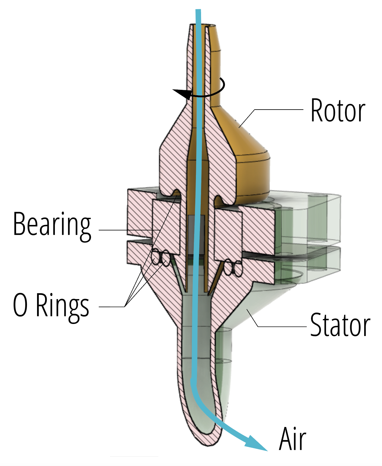
[Cross section analysis of the device]
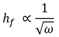
4.1 Spin Coating Theory
Generally, literature sets that the thickness of the layer spinned proportional to the invers of the square root of the angular velocity:
[Spin Coater doing its stuff well]
We know that the thickness values will follow a curve that looks like this plot:
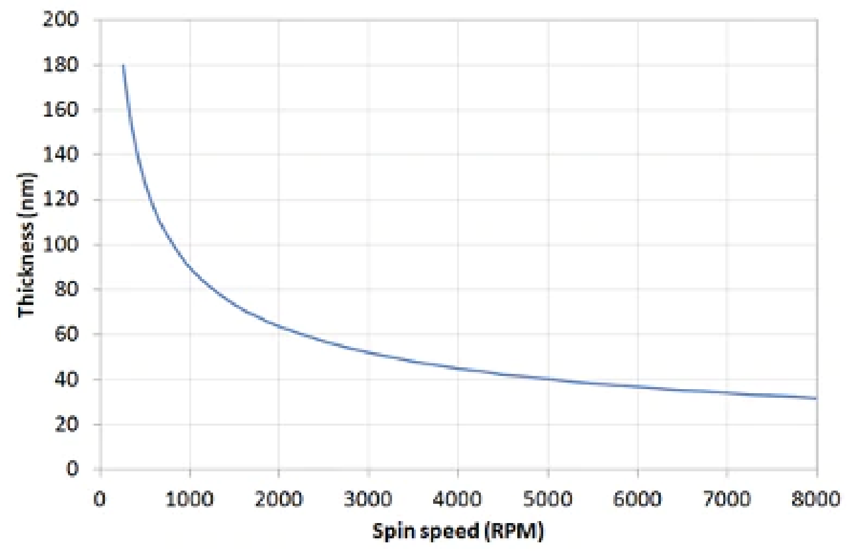
[Spin Coating: Complete Guide to Theory and Techniques, https://www.ossila.com/pages/spin-coating ]
But we might need to fit some empirical data to match values of Thicknesses if we dont want to take introduced account in our equations viscosity and time parameters.
4.1 Spin Coater Characterization with Ellipsometry
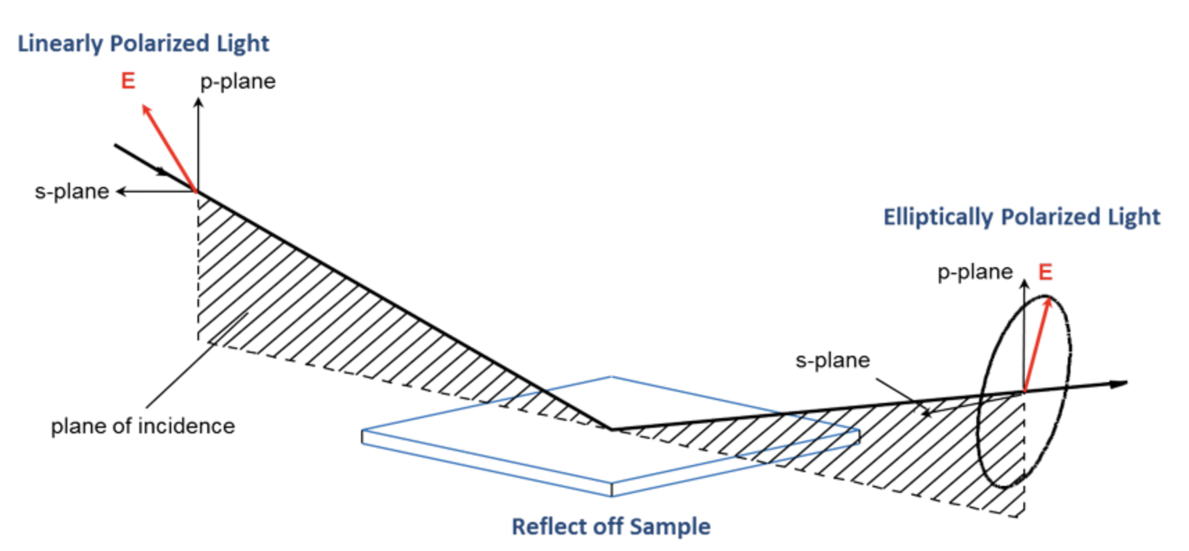
[Light Path Scheme. https://www.jawoollam.com/resources/ellipsometry-tutorial/what-is-ellipsometry ]
As we learned in my favourite chapter of PIT where we start deriving Maxwell's equations and seeing that light can be defined as an electromagnetic wave travelling through space. We can assume the orthonormality of both of the planes (electric and magnetic pulse) of it. In an euclidean space , a wave in the Z axis can be described by its X and Y components. When we force an offset (smaller or bigger than pi/2 multiples) we obtain an Elliptical Polarized light.
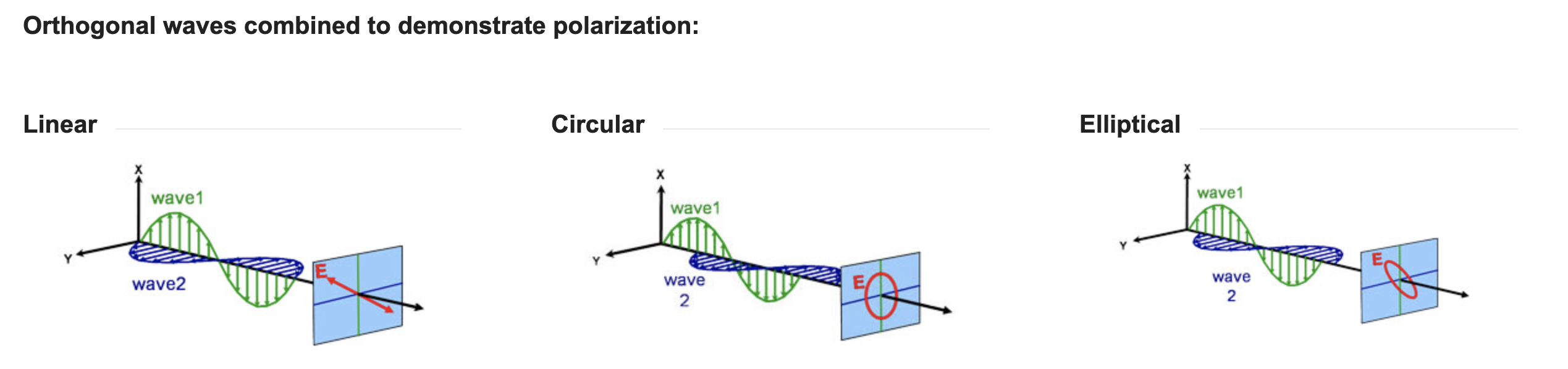
[Linear, circular and elliptical Polarized Light. https://www.jawoollam.com/resources/ellipsometry-tutorial/polarized-light]
As Maxwell equations needs to keep satisfied when the beam hits the material, incident light will reflect and refract at the interface as we saw in Chapter 9 equation 9.9.
Ellipsometers meassures the p- and s- differences from the emmiter and the receiver and translates it into thickness value of the medium reflected.
[Interferences. https://www.jawoollam.com/resources/ellipsometry-tutorial/polarized-light]
Now, using ellipsometry ourselves, after spinning some samples, we compare here the silicon wafers done by MIT Nano vs. our Fablable Spin coating method:
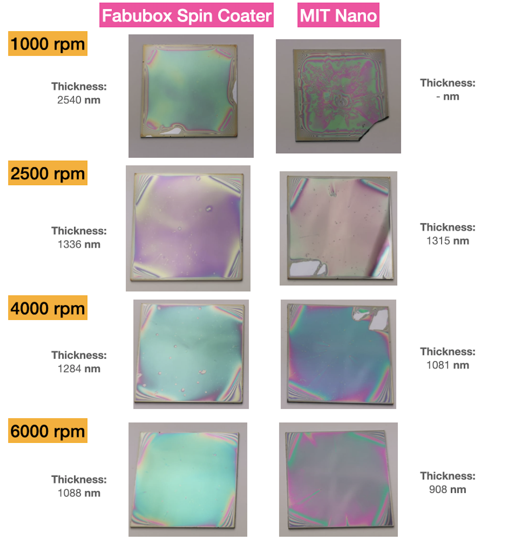
[Alfonso Parra Rubio, Jan Onchoke Tiepelt. MIT 2022]
If we look at the photoresistor datasheet, we can compare where we both are:
After spinning some samples, we compare here the silicon wafers done by MIT Nano vs. our Fablable Spin coating method:
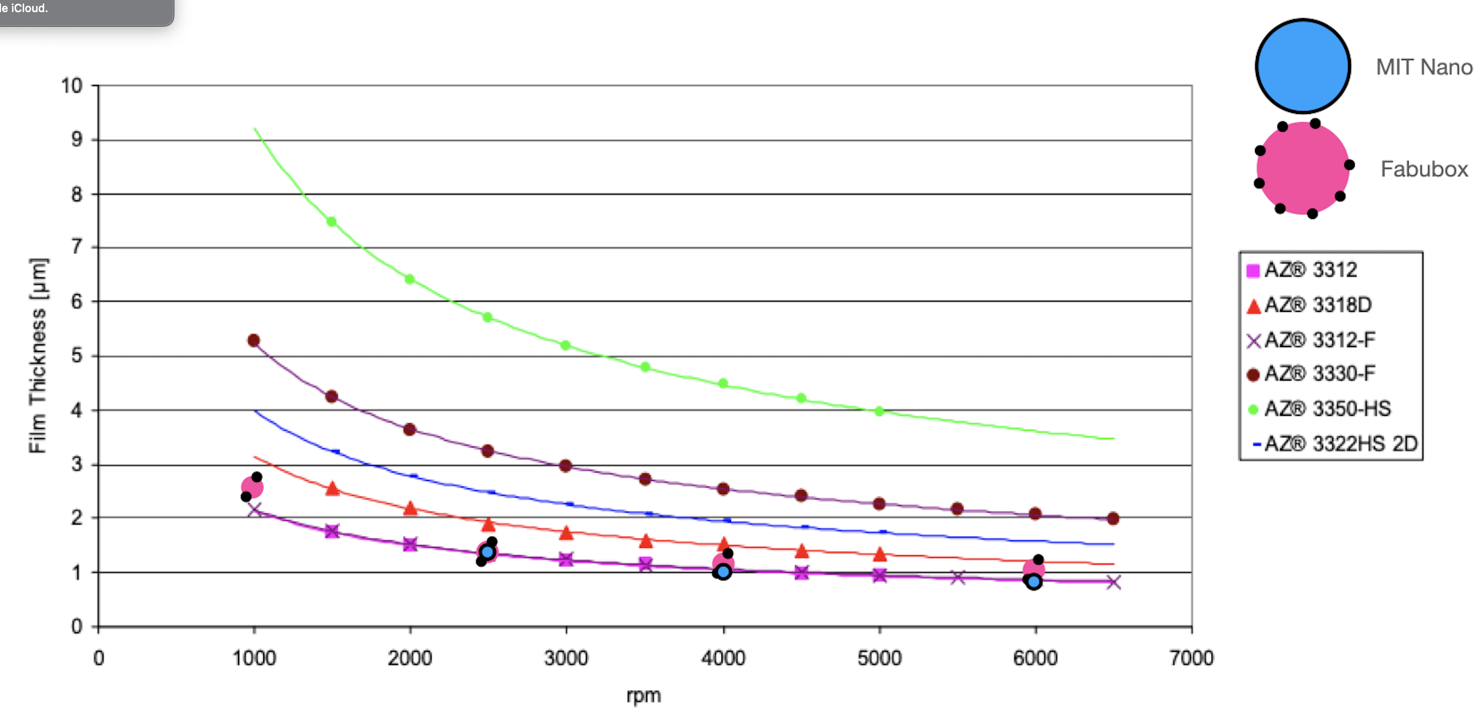
[AZ 3312 Photoresist Datasheet. https://cores.research.asu.edu/sites/default/files/2019-10/az_3312_photoresist_data.pdf]
5. Hot Plate
Many Fab processes requires a controlled baking time to makes those polymers to settle down and stabilize // rigidize ,etc. I took advantage on my 5 days at home to make a hot plate for the box and it became much more handy than I thought.
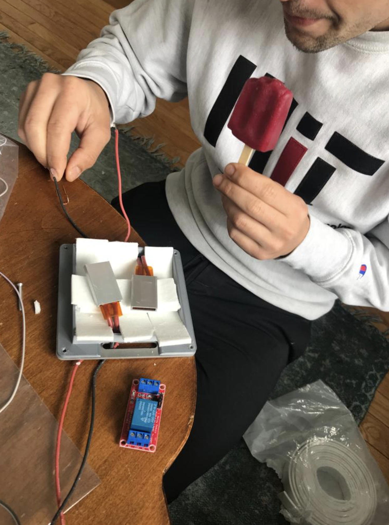
[Me with covid, a popsicle, a thermistor, filling the guts of the hot plate]
I purchased in Amazon two 50W 12V DC heaters and put it in between a thermistor. I encapsulated a sandwich composed by two aluminum 3mm plates, ceramic foam and a voltage divider with a 1k Ohms resistor and the thermistor.
Back in the lab, Jan and I added this tiny Oled displays inside the Fabubox module plate and it looks very cute as well as functional. We definitely enjoyed our own UI UX or howhever you write that.
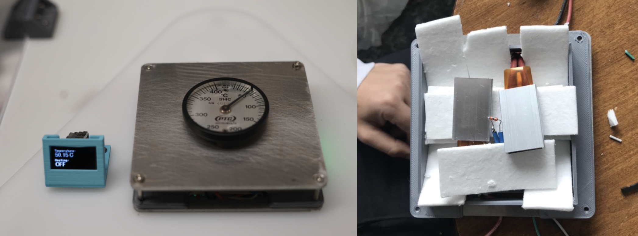
[Hot Plate assembled with a thermometer we trust. Hot plate guts]
6. Manufacturing and Characterization of Organic Solar Cells
We have seen in the theory section how inorganic solar cells works. For my final project I decided to build a P-N junction and when asked Jan, he suggested to make an organic solar cell. The main reasons why academy and industry are moving towards organin non cristaline devices are because
The downsize is that silicon still have a higher efficiency, but research is going well and they are close to almost match performances. Organic exciton values are much higher making less efficient to jump the electron - hole pair.
The polymer choosen to be a Donor / Aceptor for our process is the solution PV2000:PCBM because it is cheap, Jan have some, it is stable to be done in air (no need of removing oxigen). The stack choosen will be a glass wafer, ITO, a layer of ZnO, the polymer, MoO3, and Silver.
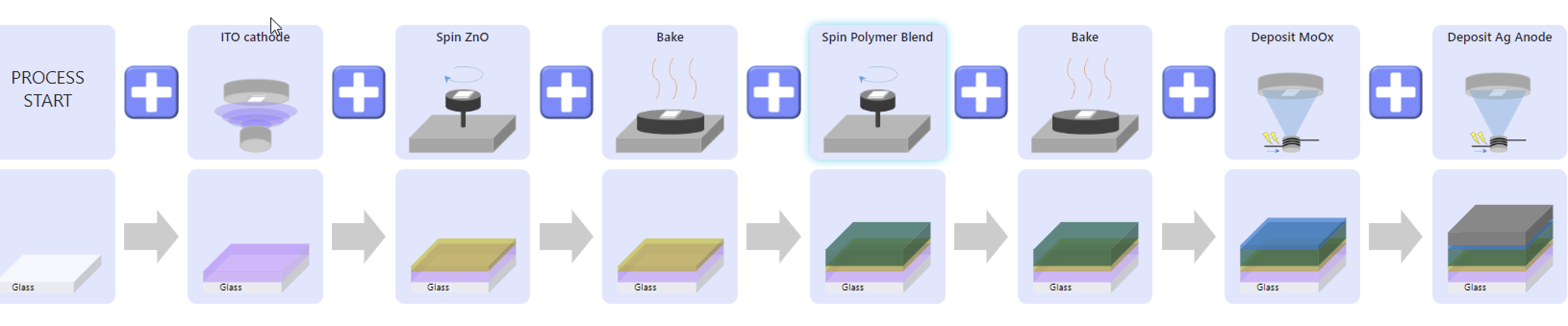
[ Fabublox process]
This architecture is called a bulk hetherojunction. This means that the P-N Junction is not defined as a straight boundary but rather, as a non super homogeneous blend. That allows to increase the area in which the donor and the acceptor interacts.
6.1 Manufacturing
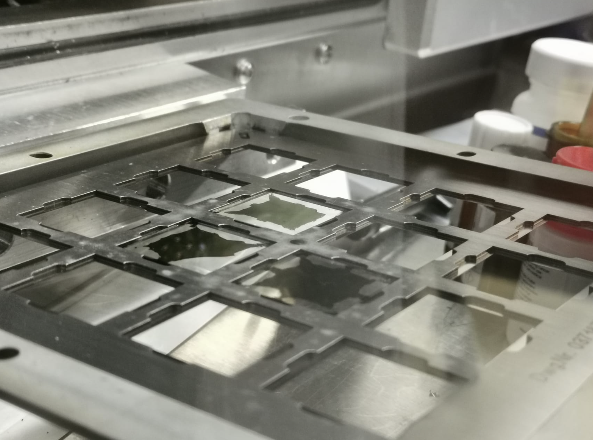
So, this is the stack of materials that we are going to (very carefully) deposit on the glass wafer: First, we used commercial patterned ITO substrates from TFD Thin Films Inc as the cathode.
[ Cristal Wafers]
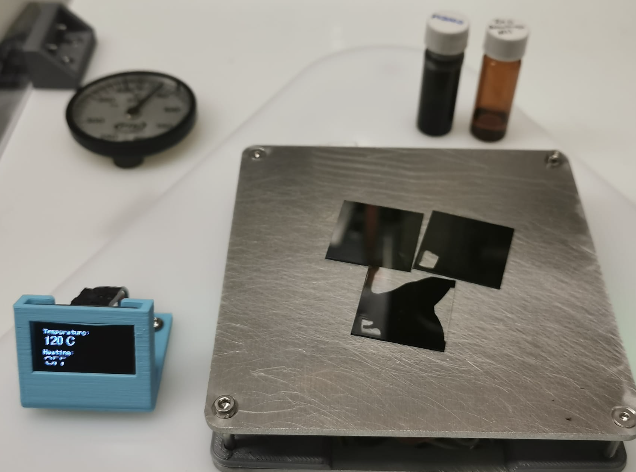
Now, we are going to spin ZnO. As we broke the first sample (luckily we had 4), we are going to spin at 3 different spins for 90 seconds 100 micro liters of ZnO. Then we will bake it 3 minutes at 120 Celsius.
The three speeds are 700rpm for Sample2, 1000rpm for Sample3 and 1300 for Sample4.
[ Cristal is transparent and ZnO also so, not much to see]
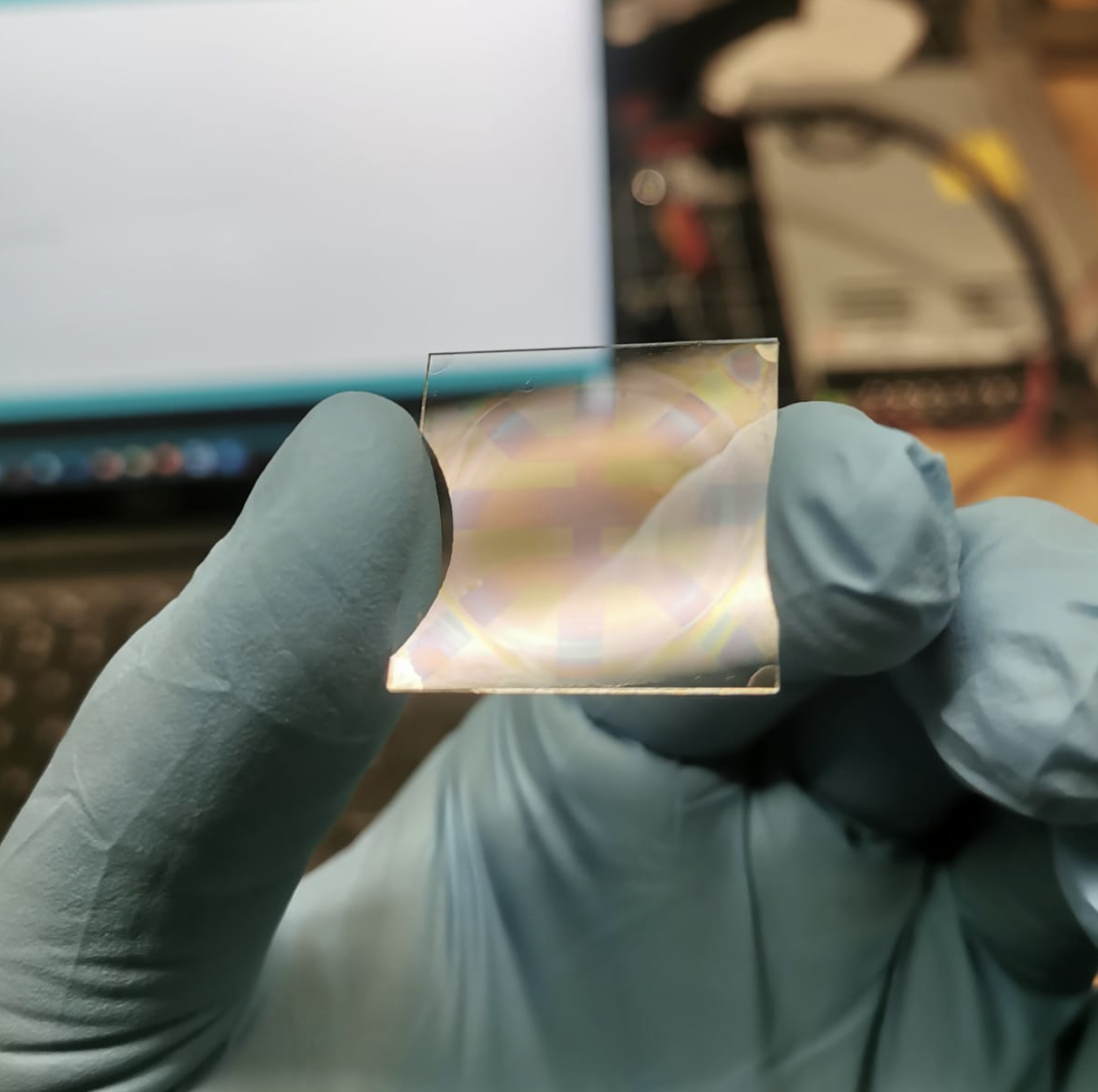
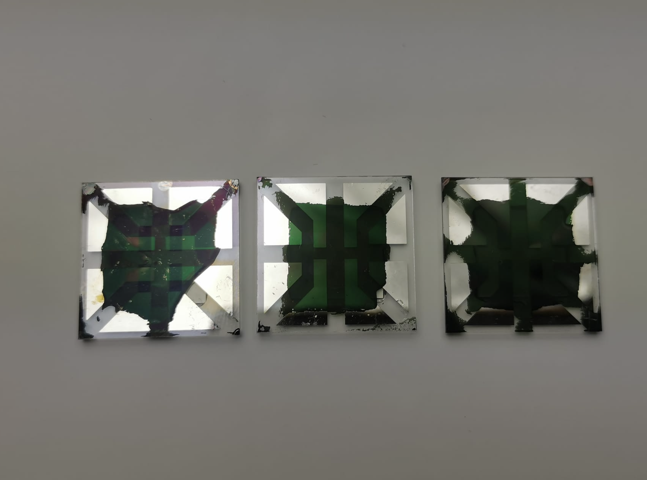
After all samples being baked, we go to deposit 200 microliters of PV2000:PCBM.
[ PV2000:PCBM is black so now we can see it. ]
[ Satisfying ]
Now, we bake them again for 90 seconds at 120 celsius and save them to be cleaned with acetone in the edges so we can hace nice contacts with the anode and the cathode.
[ Transfering. ]
[ Baked]
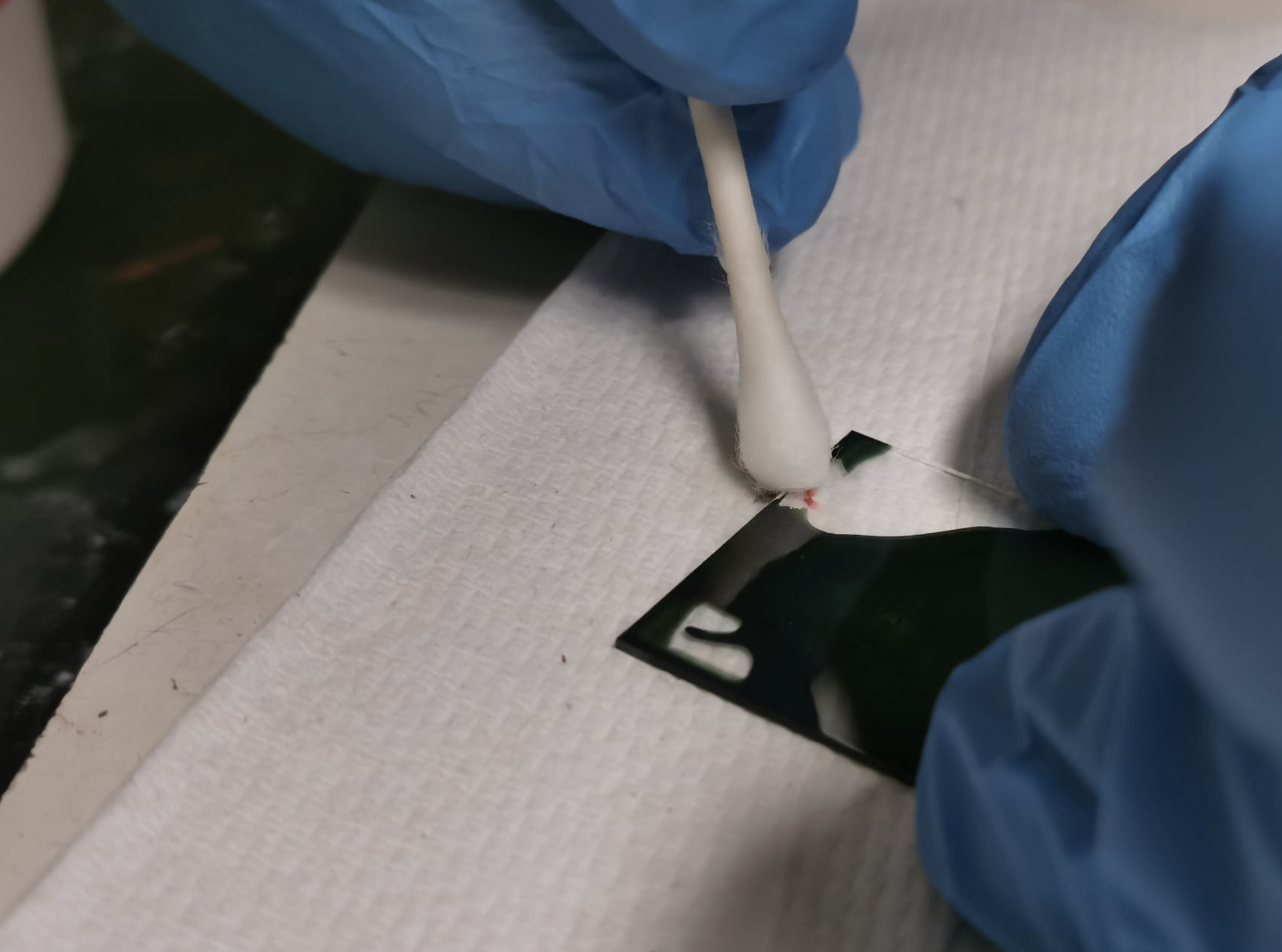
[ Accetone cleaning]
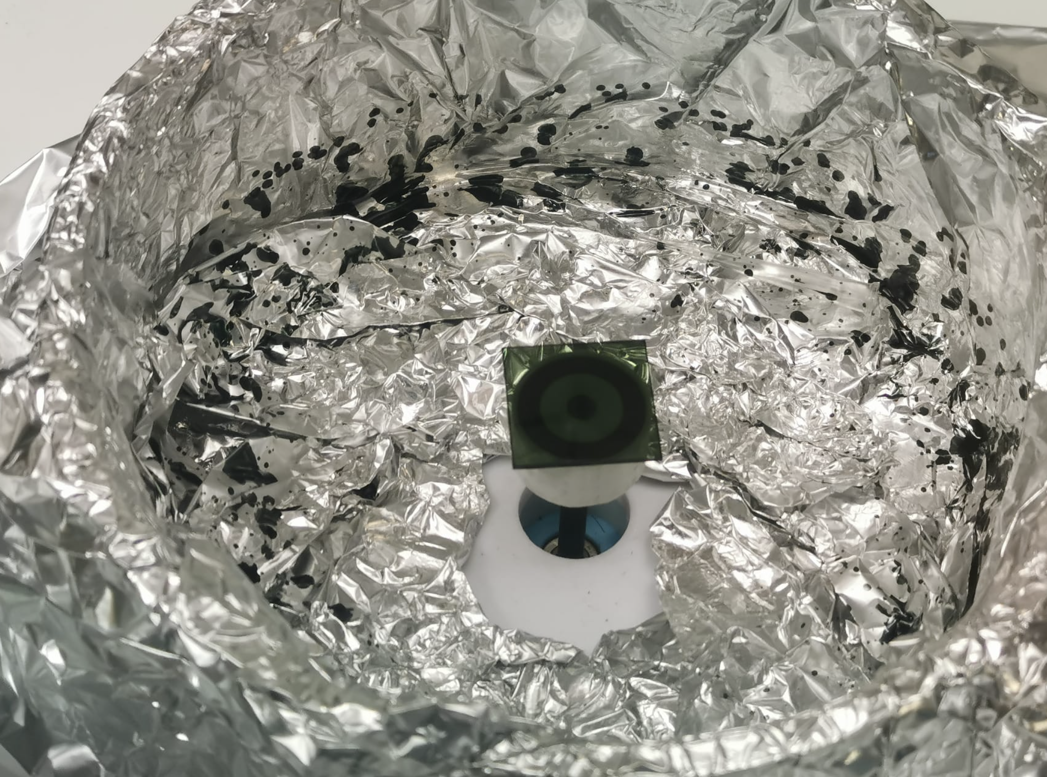
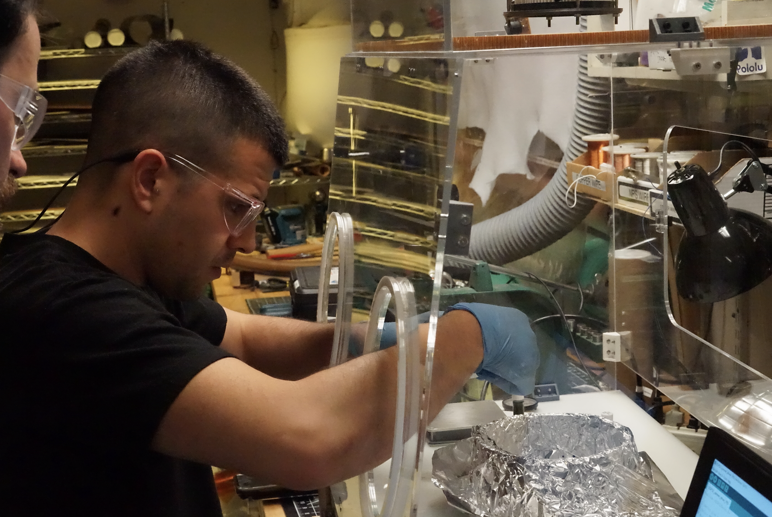
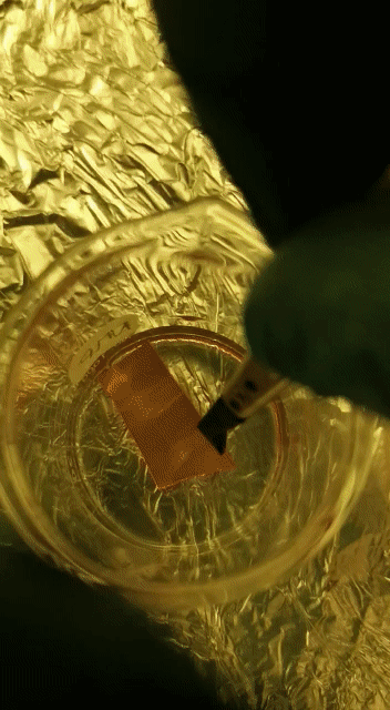
Now,we need to move out the Fabubox because the rest of the operations cant be done here sadly. Future experiments could include liquid metal ink deposition or table top vapor layer depositon.
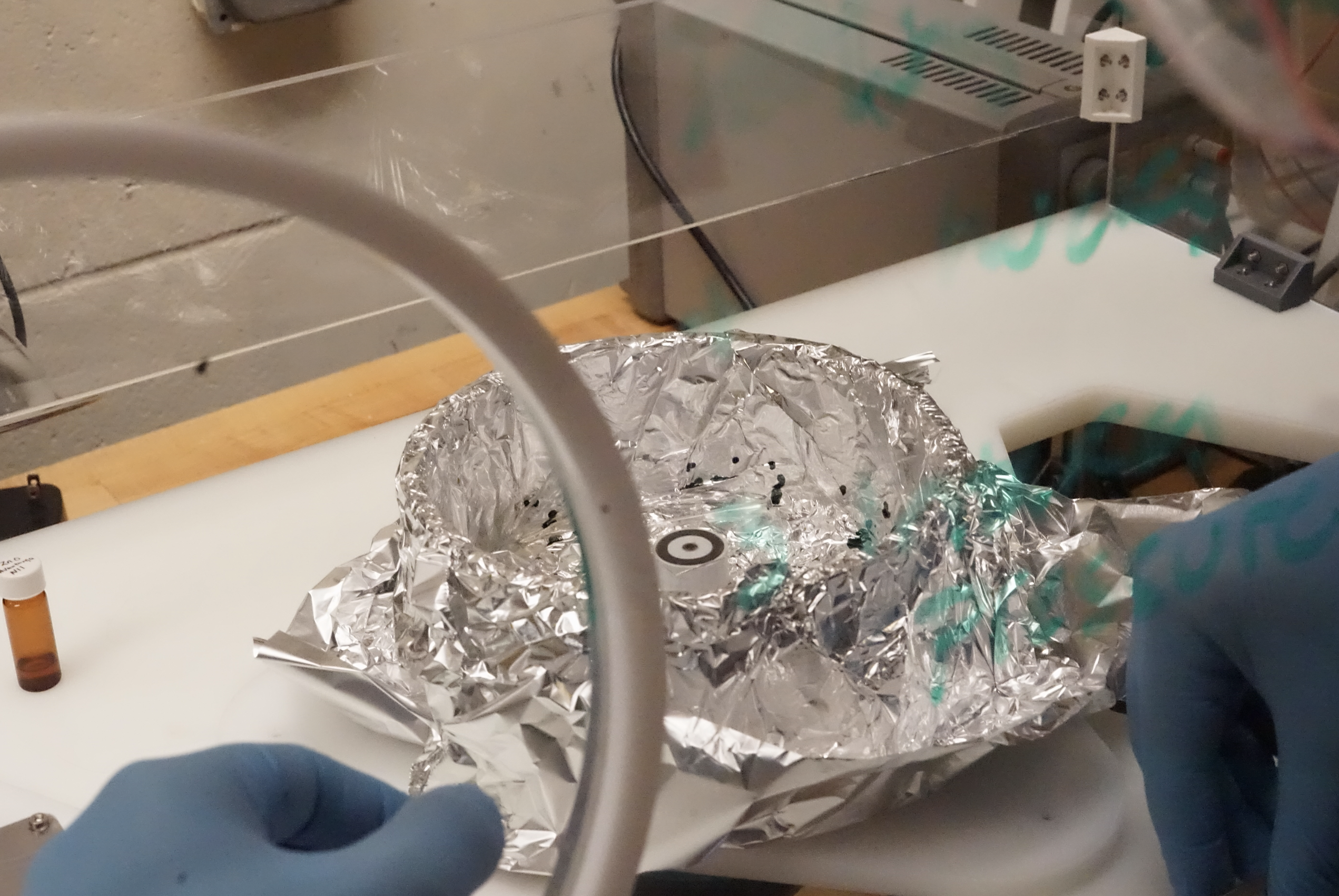
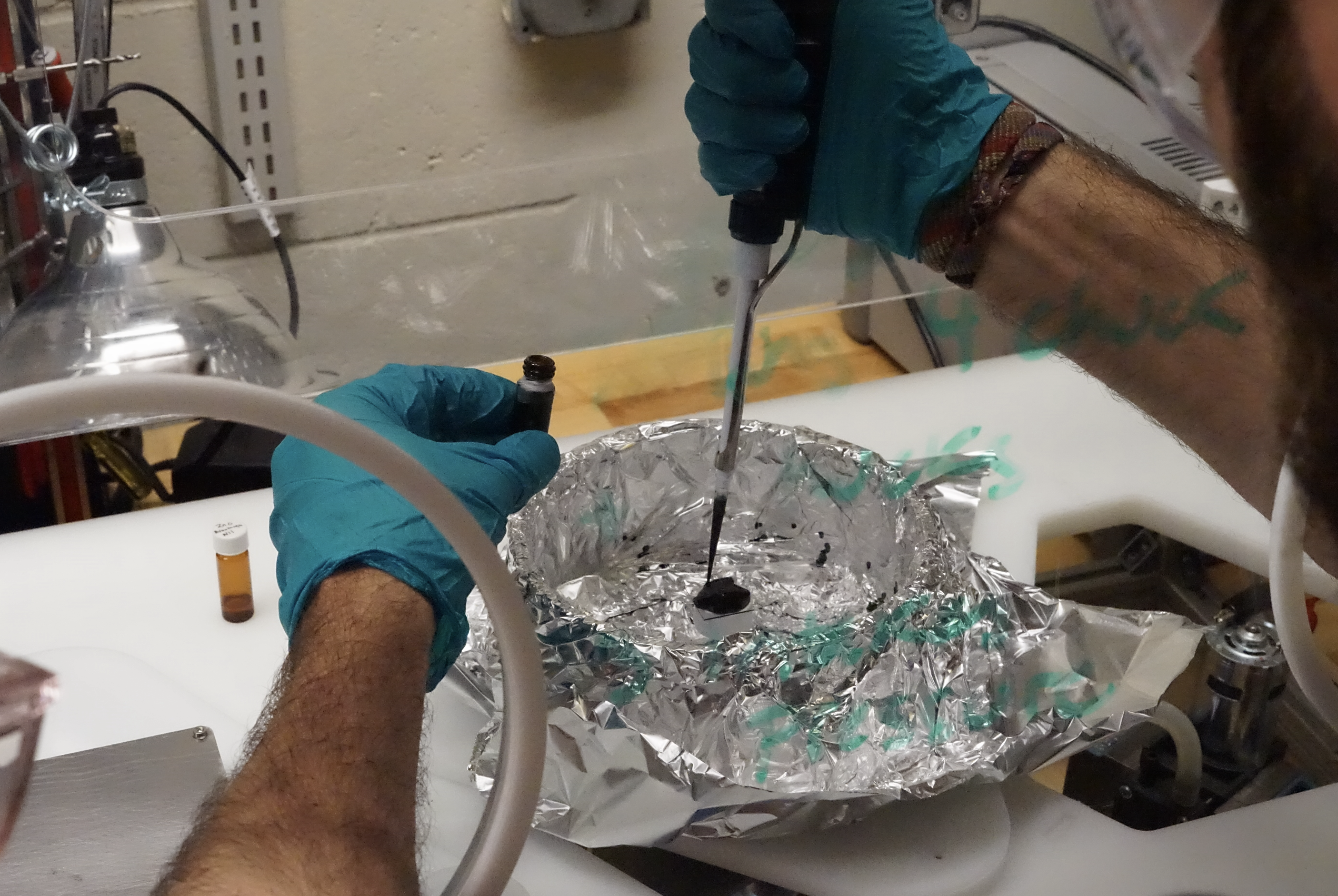
We are depositing now 50 A of MoO3 (as hole extraction layer) and 1000 A of Ag(as the anode). Jan helped me with his Angstrom Vapor Deposition machine in which, in an enviroment with a lack of oxigen, heats up metals into sublimation and deposit a thin homogeneous later over the samples as can be seen in the images:
[ Samples ready to be vapor deposited. ]
[ Samples Finished! ]
6.2 Characterization
This is exciting. We are going to characerize to main elements in solar cells. One is External Quantum Efficiency which is, given a range of bandwidths, how many photons am I hitting per area vs how many electorns I am making to flow. To do so, we go to the Optic Lab and use this amazing setting :
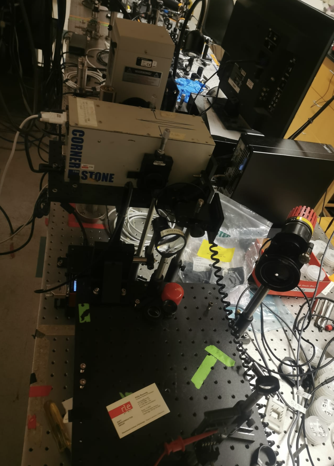
[ Optical setup ] The setup is composed of a Tungsten lamp with a white spectrum that covers all the visible, pass through a monochrometer, pass through a chopper wheel that will feed the reading freq of the lock in amplifier, and finally hits the solar cell. We will read voltage and amps of the cells being hitted at wavelengts from 400nm to 800nm.
.png)
[Meassured External Quantum Efficiency of the Organic Solar Cell. All samples were exposed to wavelengths from 400nm to 800nm ]
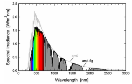
[Solar Spectrum. https://www2.pvlighthouse.com.au/resources/courses/altermatt/The%20Solar%20Spectrum/The%20global%20standard%20spectrum%20(AM1-5g).aspx ]
Next, comes the I-V characterization. I could not get access to MIT Nano so Jan did this experiment.
First, we are going to read the cells as diods, with no photon excitation. And It should behave as a perfect diod. We can check here if we have leakage current.
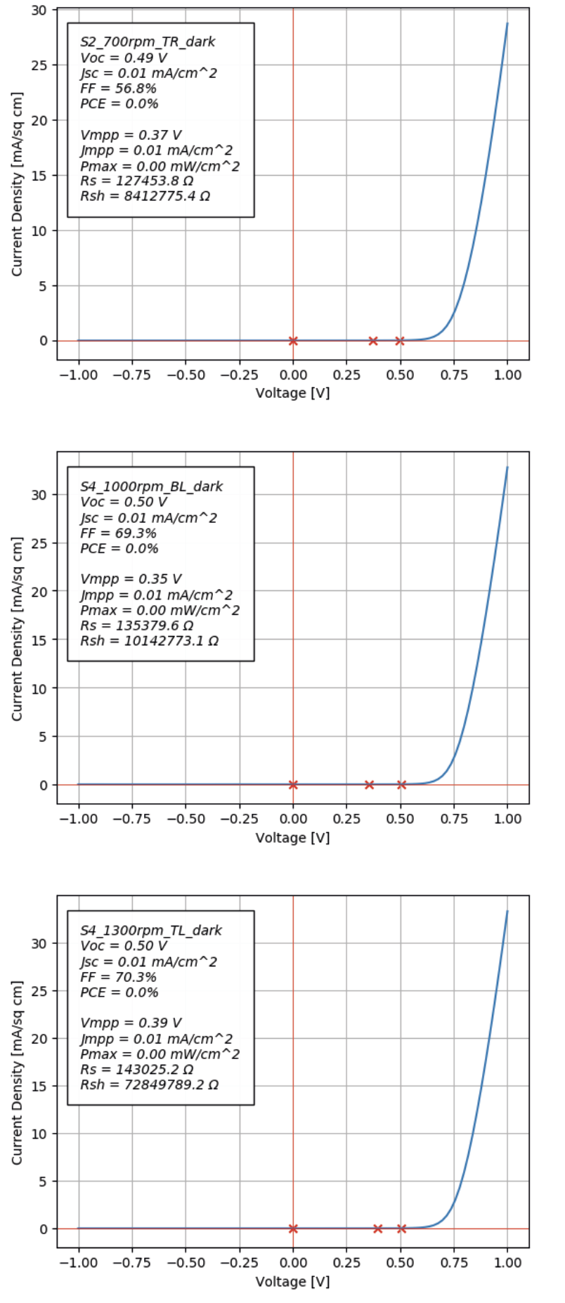
[ Dark I-V ] Now, exciting it with light we see the same curve but with a offseted voltage, which is behaving as a solar cell!
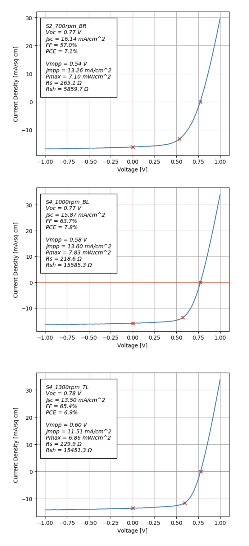
[ Optical setup ] We see that they behave incredibly well, as theory. We have receive compliments from solar cell researchers!
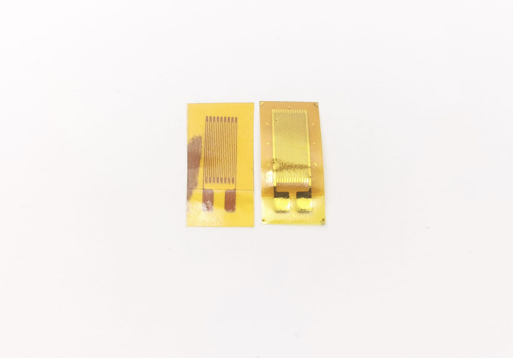
7. Strain Gauges and other flex PCBs
Wait, there is more!
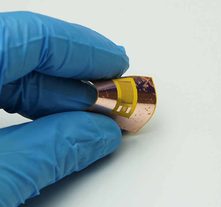
[Me holding a strain gauge we made in the Fabubox. One of the cutest things ive done]
Through this process, we realized that this box can increase drastically accesibility to fabricate in house and with a low cost devices that today are much likely to be purchased on the internet. For example, strain gauges, flexible PCBs, piezoelectric sensors... So we are showing here a semi hacky method to build your own strain gauge stickers.
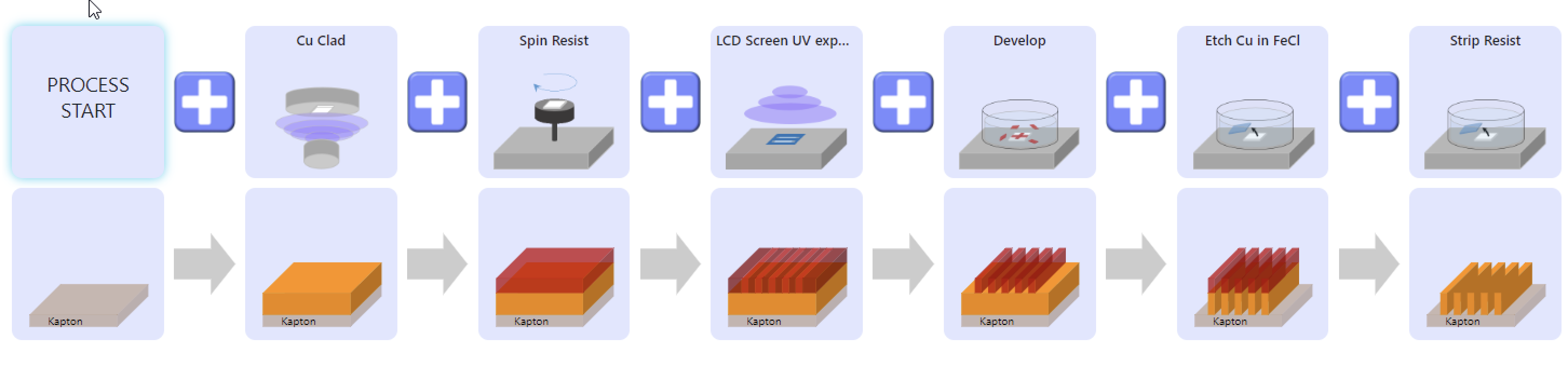
Lets take as an example a strain gauge. This method is exactly the same as the one to make a flex PCB. We just want to push the limits of how small we can go. As we said before, all electronics starts with a spinnig process. We took Dupont Pyralux, which is a material composed by 18 microns of Kapton and 18 microns of copper.
[Mars3 thinking its printing this but its not. Guapisimo]
I took the chunk I build for flexible substrates, in which I transmit with porus the vacuum and placed a large sample of Pyralux. I placed photoresistor AZ3312 and spinned for 40 seconds at 3000rpm.
[Flex at 3000rpm is impressive]
Once spinned we need to make our traces. To do so we used a Elegoo Mars3 LCD printer as a maskless masking process?. We are going to use the monochrome 4k LCD screen to let UV light touch only what we want to degrade! This allow us to go as smaller as the pixel level is. For a 6 inches 4k resolution screen, the pixel distance is 35 microns. I did a parametric design of strain gauges based on jumps of 35 to 35 microns and, it worked. We send the printer an STL with the circuit we want to mask.
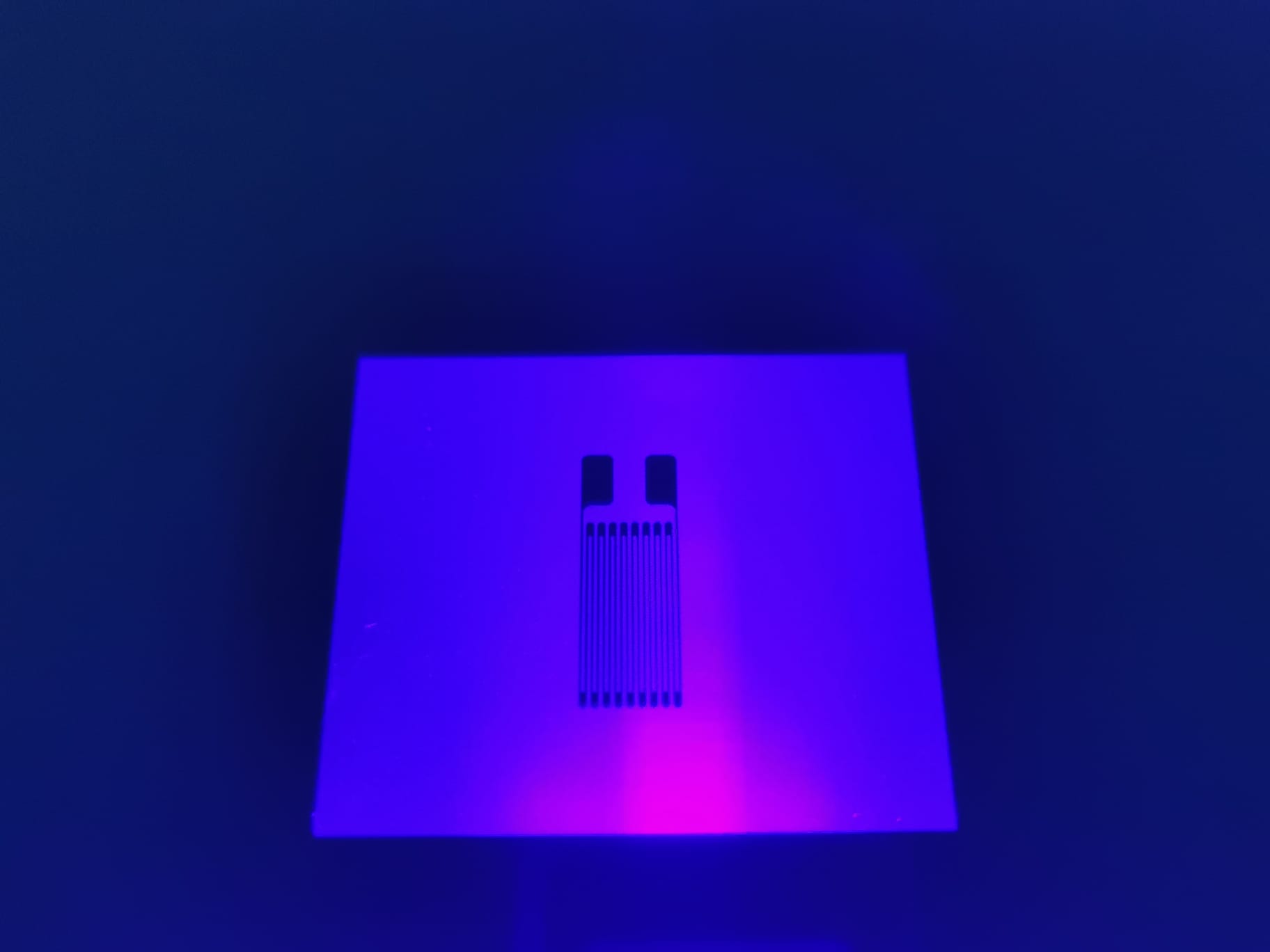
[Mars3 thinking its printing this but its not. Guapisimo]
Once we have masked the samples, we develop the non-healthy photoresistor.
[Developing]
And after that, we take Ferric Chloride and make a classic etching process to remove the exposed copper while keeping the
Then, I installed the loadcell in a flex aluminum plate and just meassure resistance. IT WORKS!
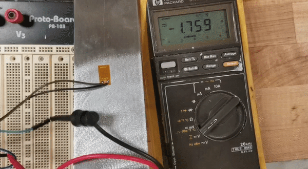
[The voltimeter can tell the voltage diff over a Wheastone Bridge]
And just to compare, take look to this omega loadcell and our in house one.
[Left, Fabubox,. Right, Omega]