Week 5 - Electronics Design
This week was dedicated to learning how to use Electronics Design Tools. I am completely new to electronics. Fortunately, however, I had worked ahead a little bit and visited the PCB Making Training at the MIT Eletronics Mezzanine, part of Project Manus (their student-run makerspaces).
KiCAD
KiCAD is an open-source EDA software. It is a suite of programs that allows you to design schematics, PCBs, and generate Gerber files. It is available for Windows, Mac, and Linux. It’s a little convoluted since it merged multiple tools into it over time, so that certain functionalities are not very intuitive to find. However, it is free and open-source, and there are many tutorials online.
Eagle
Eagle is a tool that used to be free but has since been bought and integrated into Fusion 360. That makes it really nicely integrated intot the Fusion landscape, but it also means that it is no longer free. I decided to use it for my weeks, since I want to learn Fusion 360 well, and I will be using it for my final project. I will show the process of designing a board in Eagle in the weekly documentation.
Schematics
The first step is to design the schematics. This is done in the Eeschema program. You can add components from the library, and connect them with wires. You can also add labels, which are useful for the PCB design.
PCB Design - Footprints
The next step is to design the PCB. This is done in the Pcbnew program. The first step is to assign footprints to the components. Footprints are the physical representation of the components on the PCB. You can find the footprints in the library. You can also create your own footprints, but this is a little more advanced. However, since we did have custom components in our library, we also needed to import the custom footprints. This is done by going to Preferences -> Manage Footprint Libraries -> Project Specific Libraries, and adding the custom library.
PCB Design - Placement
The next step is to place the components on the PCB. You can do this manually, or you can use the auto-placement tool. The auto-placement tool is not very good, so I would recommend doing it manually. You can also use the auto-routing tool, but again, it is not very good, so I would recommend doing it manually.
PCB Design - Routing
The next step is to route the traces. You can do this manually, or you can use the auto-routing tool. The auto-routing tool is not very good, so I would recommend doing it manually. You can also use the auto-routing tool, but again, it is not very good, so I would recommend doing it manually.
PCB Design - Design Rules
One important thing when designing PCBs is to set design rules. Design rules determine the minimum trace width, minimum trace clearance, minimum via diameter, etc. This will essentially determine how close routes can be to each other, and how small they can get.
That is it for the EDA design with KiCAD! Now on to the real assignment for this week.
Assignment: Solving my MAX7219 LED Routing Problem with Hardware
Initially, I was hoping to build a board for an initial prototype for the flip dot display. Marcin Saj even has these beautiful schematics in his documentation.
However, they unfortunately, seemed quite advanced. When I asked Quentin (TA) about it, we discussed my final project and he suggested not doing a magic mirror, as the class wasn’t really made for those types of projects that require many of these manufactured items. Also, the electronics seem to be really complex for this one.
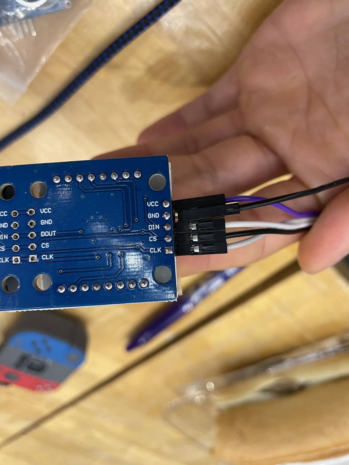
When I showed him my MAX7219 LED from week 3, he suggested something much simpler: a board that would solve my routing problem. I had been using a breadboard or direct wires for the MAX7219 LED, and he said it would be beautiful if I could hide that complexity in a custom board, attached to the back of the LED. Then I could wrap the little display in a cute shell. After some deliberation (it seemed a bit too simple), I decided to go for it.
Concept: Totoro LED Display
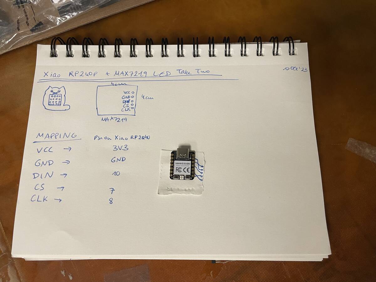
I thought of Totoro or a cat or bunny as a cute shape for the display, which could live in its belly. Going back to Embedded Programming week, I confired the routing between the MAX7219 and the Xiao.
Designing the Board
This time, I decided to use Eagle, which is now integrated into Fusion 360. I want to learn how to use Fusion well, so it makes sense to learn Eagle. There is a great tutorial on the CBA “Machines That Make” website, which I highly recommend. It basically teaches you all you need to know for this week’s assignment.
Now, onto the LED shield.
Schematics
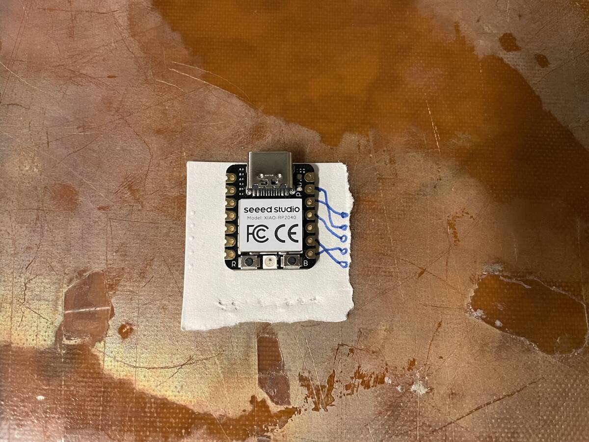
The schematics were quite straightforward: I just needed to import the Xiao RP2040, which is included in the fab library. Then I needed 5 throughholes. That’s it.
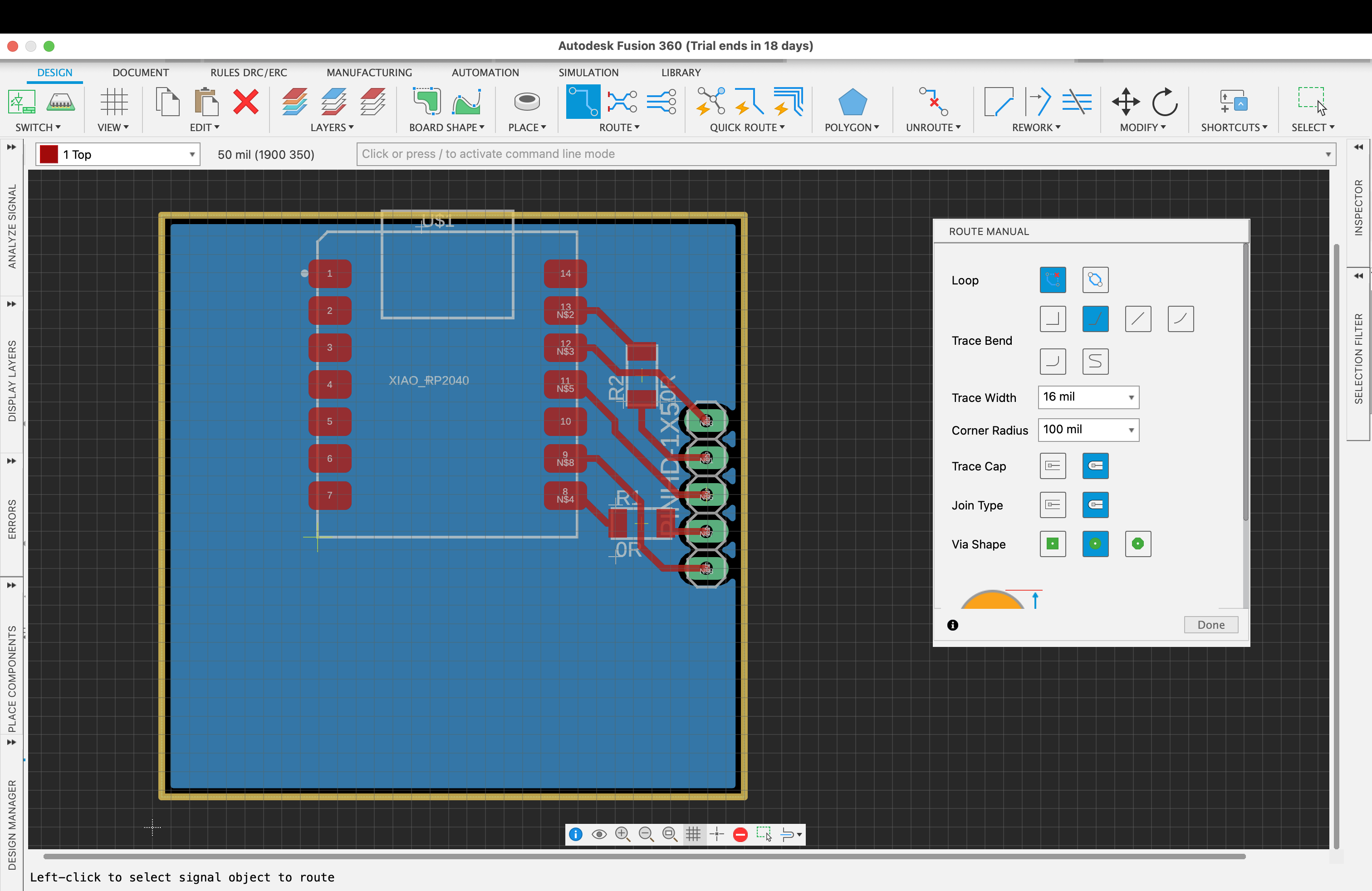
Board Design
Two challenges here:
-
The routes cross. This is not allowed. However, I could not route around the throughholes because they live on the edge of the MAX7219, so there was no space there. The trick (explained in the tutorial video) is to use a 0 Ohm resistor to route underneath the resistor. This way is particularly useful for rapid prototyping PCB milling.
-
Missing footprints for the MAX7219. That meant I had to measure the board size by hand and figure out where to place the througholes.
After having first designed the route traces, I held the MAX7219 PCB against the screen, I could see that the pinouts definitely aligned - good! Eagle’s grid is actually real-sized. However… the size of my outline… wasn’t correct. It was somewhat too large. So I remeasured the MAX7219 with a ruler to find out that the actual size was 3.2cm instead of 4cm (never trust the iPhone Measure app to mm again). Oops.


So back to Eagle to change the outline size. I found the easiest way to do this is to adjust the grid to the metric you’re using and drag the outline along.
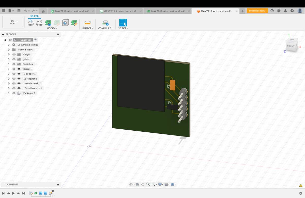
Simulating
In Fusion, we can even easily simulate how the board would look.
Exporting
The way of exporting depends on the milling tool you want to use.
Gerber is the standard format when sending out a PCB design to a manufacturing house. It is a set of files that contain the information about the layers, the traces, the drills, etc. It is a standard format, so it can be read by any PCB manufacturer. However, it is not a format that can be read by a milling machine. For that, you need to export the G-code. G-code is a set of instructions for the milling machine. It is a standard format, so it can be read by any milling machine.
I used the Bantam Tools Desktop PCB Milling Machine, which accepts Gerber and let’s you turn it into G-code. I also exported the drill file, which is a .txt file with the coordinates of the holes.
However, for using the Roland Milling Machine, we use MODS, which is a custom program written by Neil. I haven’t used it yet, but I will try it out next time at the REEF Makerspaces at Harvard.
use script for Fusion: run singleImages Electronics Design Tools HTMAA 2022
(This documentation was written with the help of Github Copilot)