final project - DICE analytical, numerical, experimental
Table of contents
motivation
the current DICE geometries (4BI, 4BIc) are approximately 5x5mm tiles at 5.66mm or 8mm pitch, depending on how you look at it.
although there is merit to introducing heterogenous integration (HI) to replace breadboards and PCBs +- IC packaging (eg roughly electronics packaging levels 2 and 1, respectively), the eventual goal is to compete with existing HI solutions targetting packaging at level 0, or chiplets.
a key metric towards scaling down feature sizes is length of wires, and subsequently inductive and capacitive parasitics. these EM simulations will roughly aim to simulate how these parasitics change as features are scaled down, and how different configurations impact performance.
note that although scaling simulations may simplify geometry assumptions, it is likely that competing design requirements (and physics) will likely dictate different solutions for different regimes.
05.16 - analytical
due to time, simulation and experimental are future work.
analytical performance projections
04.24 - comsol study setup
geometry
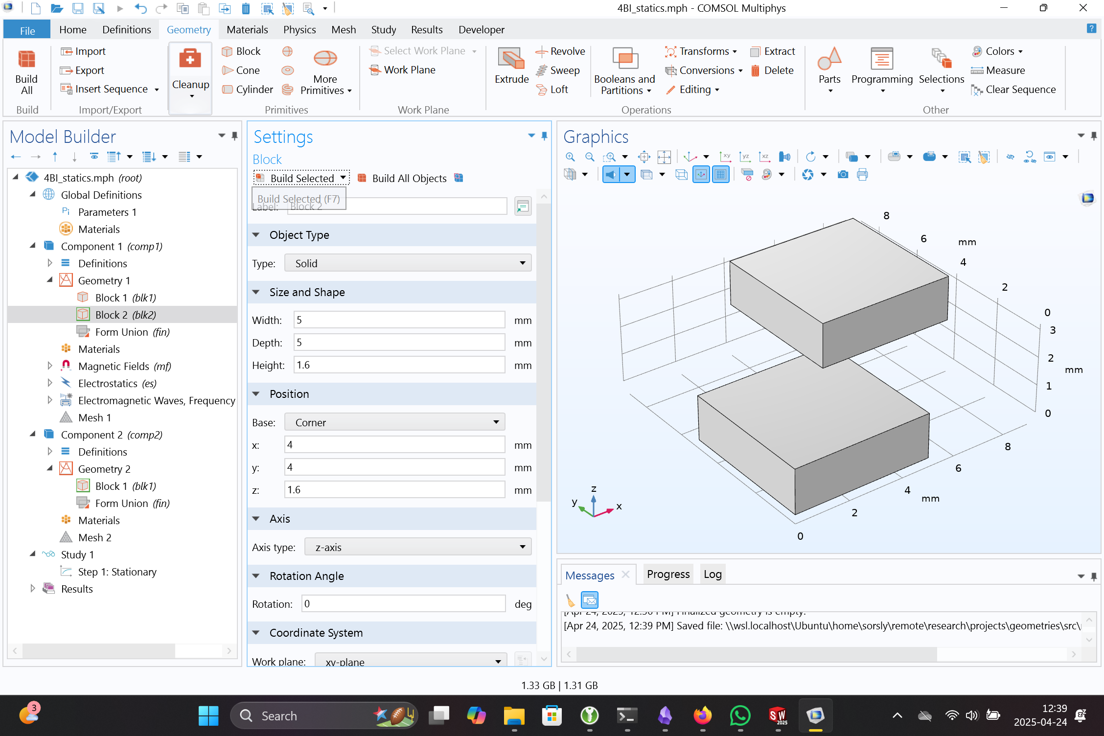
initial geometry is two 4BI tiles and their interface using the built-in boolean objects. ideally we import CAD from 4BI (or 4BIc) and work from there, but this takes 30 seconds and importing will take much more.
configuring model(s)
configuring a project template (with some help from gpt) including the following solvers:
| Physics Interface | Study Type | Purpose | Notes |
|---|---|---|---|
Electrostatics (es) | Stationary | Extract parasitic capacitance | Apply voltages to conductors, get C-matrix |
Magnetic Fields (mf) | Stationary | Extract parasitic inductance | Inject currents or define loops, get L-matrix |
Electromagnetic Waves, Frequency Domain (emw) | Frequency Domain | Simulate crosstalk and coupling | Extract S-parameters, sweep across frequency |
(tentative) study space:
| Study Name | Add From | Interfaces to Include | Solver Purpose |
|---|---|---|---|
| Capacitance Study | General Studies → Stationary | es only | Static voltage distribution for C |
| Inductance Study | General Studies → Stationary | mf only | Static current loops for L |
| S-Parameter Study | General Studies → Frequency Domain | emw only | Wave propagation and crosstalk |
(tentative) mapping of interfaces and studies to useful values:
| Quantity | Physics Interface | Study Type | Postprocessing Method | Units | Notes |
|---|---|---|---|---|---|
| Capacitance Matrix (C) | Electrostatics (es) | Stationary | Use Electrostatics → Capacitance Matrix or compute Q/V | F (Farads) | Apply potentials to conductors, integrate surface charge |
| Inductance Matrix (L) | Magnetic Fields (mf) | Stationary | Use mf domain: compute stored magnetic energy W = ½·L·I² | H (Henries) | Inject known current, extract magnetic energy or use mutual inductance expression |
| Characteristic Impedance (Z₀) | mf + es | Stationary | Compute Z₀ = sqrt(L/C) | Ω (Ohms) | Only valid in quasi-TEM mode lines |
| Crosstalk (S21, S12) | EM Waves (emw) | Frequency Domain | Use S-parameter port results, extract S21, S12 | dB or unitless | S21 (forward crosstalk), S12 (reverse) between aggressor and victim |
| Near-End Crosstalk (NEXT) | EM Waves (emw) | Frequency Domain | S21 at the near-end port (input side of victim line) | dB | Measures direct capacitive/inductive coupling |
| Far-End Crosstalk (FEXT) | EM Waves (emw) | Frequency Domain | S21 at far-end port of victim line | dB | Measures propagation-induced coupling |
comsol
- Jiaming helped me install
- also, I found there are dedicated chiplet simulation tools:
- https://www.cadence.com/en_US/home/explore/what-is-3dic.html
- https://www.cadence.com/en_US/home/solutions/3dic-design-solutions.html
scoping
given the motivation, let’s assume the 4BI geometry is retained through multiple regimes. the geometry should be evaluated for each key electronic packaging level:
- level 0 device level: 5nm, 100nm
- level 1 IC packaging level: 5um, 500um
- level 2 PCB level: 5mm