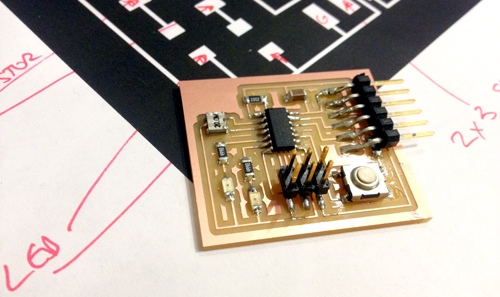
A WINKING LED CIRCUIT BOARD
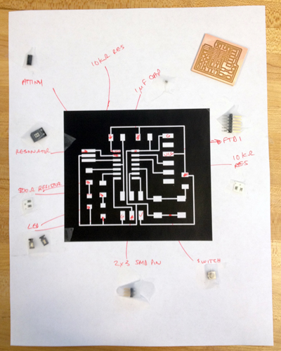
WHAT ALL OF THE PARTS ON THE WINKING LED CIRCUIT BOARD DO AND WHY THEY ARE WHERE THEY ARE:
|
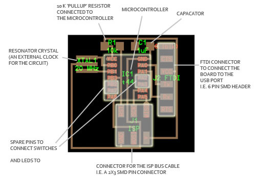
- Microcontroller: this is what controls the parts on the board and is programmed from the computer
- 'Pull-up' resistor: this 10K resistor to keep the power into the microcontroller steady near VCC or zero (this needs to be connected to the VCC pin)
- Capacitor:
- Resonance crystal: this is an external clock for the circuit (this needs the input traces to be connected to two pins on the board and the ground trace to the GND circuit)
- SMD Bus Connector: Takes in information from the FabISP and connects it to certain pins on the Microcontroller to program the board. (This needs to be connected to VCC and GND on the respective pins on the Microcontroller, and the other pins need to be connected to free input and output pins)
- FTDI Connector: Connects the circuit to the computer to read in the program and power the board (this needs the VCC and GND pins to be connected to the respective VCC and GND circuits on the board, and the Tx and Rx pins to be connected to two free pins on the microcontroller)
|
HOW TO DESIGN A CIRCUIT BOARD
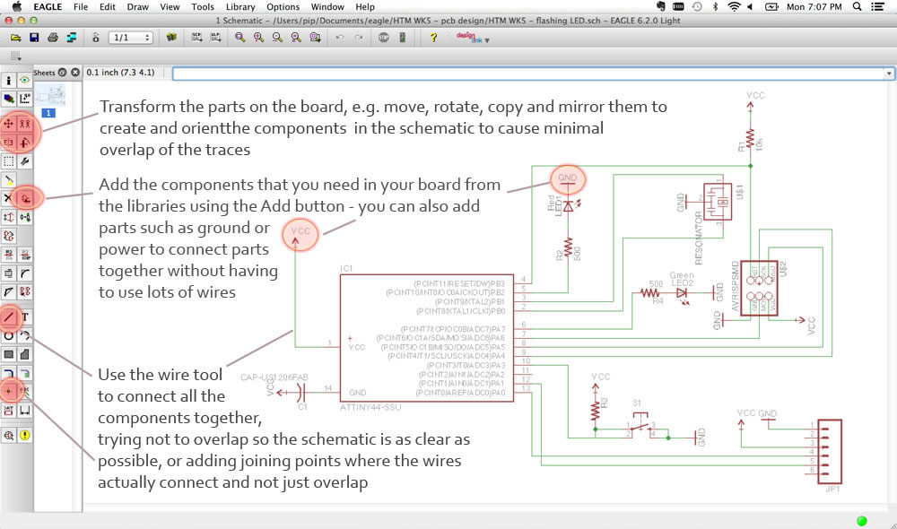
1: USE EAGLE TO DESIGN YOUR CIRCUIT SCHEMATIC
Eagle software is a pretty convenient software for circuit design and I found it quick to pick up the basics. Open a new project with a schematic and board (important to do this at the same time as they are not linked!) and start designing:
- Add all your conponents by using the add button - this opens up a window to view all the libraries you have installed from where you can add parts to your schematic (add the fab and SparkFun libraries)
- Adding parts such as GND and VCC (from the SparkFun library) to pins which are connected to VCC or GND can help connect all the parts which need to be connected to either the VCC or GND circuits without having to have lots of wires crossed over
- Use the transform buttons such as move, rotate, copy and mirror to position your components on the schematic so that it looks the clearest
- Use the wire tool to connect all the components together - where there are overlapping AND connecting wires, be sure to add a connector point so that the schematic knows the wires are connected
|
 |
|
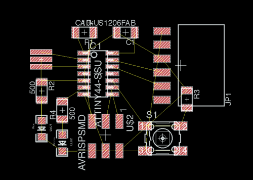
2: USE YOUR SCHEMATIC TO LAYOUT YOUR CIRCUIT BOARD
If you opened a board at the same time as the schematic, it should have linked the two together. The connection points in the parts you added into the schematic should show up as red rectangles in the board window and the connections and wires joining the parts together as yellow lines. You need to rearrange the components on the board to the layout that you want and draw traces so that they don't overlap
- Use the transform tools similar to the Schematic window to reposition and rotate the components around the board so that they cause minimal overlapping of traces
- Once you've got the parts arranged in the most efficient pattern, it's really simple to draw the traces by using the Autoroute button:
- Ensure you are drawing on the trace layer (go to Hide/Show and choose the Trace layer)
- Click on the yellow line ending at the connector of one part - this should highlight all other parts connected to it (based on the circuit design in your schematic) in bright red and help guide you to draw traces to these parts
- Repeat this until you have no yellow lines left on your board
- Using the Info tool and clicking on the traces will show you the properties of the traces and allow you to change the thickness of the traces (I used 0.12mm as the minimum resolution of the Modela is apparently 0.1mm)
- Go to the Dimension layer (Hide/Show button) to draw the outer dimension, i.e. a rectangle, to cut out the board
|
 |
3: EXPORT .PNG FILES TO MILL OUT THE CIRCUIT BOARDS
- Use the Hide/Show button to show the different layers
- File > Export > Image
- Make sure to change the resolution to 1500dpi for the Modela to be able to mill the board out accurately
- You then need to edit these images in Photoshop to remove any colour information (i.e. make them Greyscale), make the traces image white on black background and the dimension black on a white background, crop them or add other text/images - be sure to keep the resolution at 1500dpi!
|
|
4: MAKE THE CIRCUIT BOARD AND STUFF IT
This was a similar process to when I made the FabISP:
- Position board on flat bit of bed and put a 1/64 end mill in
- Open make_png_rml in Terminal on the Modela computers
- Upload traces png
- Change default to 1/64
- Make path
- Set origin and make sure end mill is touching the surface of the board all over the board
- Make rml
- Send it!
- Repeat for 1/32 end mill and dimension png
- Wash the board
This time I had a few problems with the make_png_rml program not wanting to talk to the Modela and then not wanting to send my png:
- Restarting and making sure the computer was plugged into the right port on the Modela fixed the communication problem
- I tried re-exporting my png files in the GIMP program on the Modela computer and that seemed to fix the problem of the make_png_rml program not understanding my png - maybe there was some file corruption or resolution mis-match when I exported the files on my own version of GIMP
For stuffing the board, this time I used Laura's tip of taping your components to a piece of paper. I actually printed out the trace diagram and labeled what each of the parts and important connection points were, so it would be very clear what parts of which component I needed to solder to my board. |
|
5: CHECK THE CIRCUIT BOARD FOR SHORTS
Before programming the board (in a couple of weeks), I checked that there were no shorts with my multimeter.
|