Step 1: Setting up Eagle
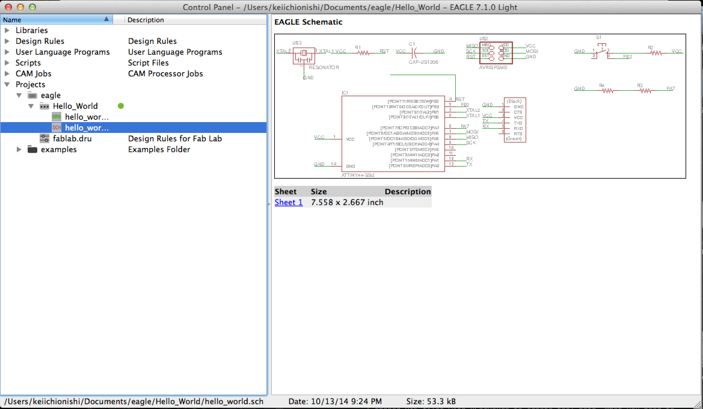
I installed Eagle for MacOS. To design hello_world board I downloaded a library(fab.lbr) and put it under a folder "lbr" in "Eagle" application folder. Next step was choosing directory of libraries. I chose Option>Directories>Libraries>browse, then chose the location of fab.lbr. Now I am ready to use the library. Next step is creating new project under eagle folder. You go file>New>project, then you will see new folder is created under eagle folder. You go file>new>schematic, then you are ready to start designing the board.
Step 2: Designing board using schematic
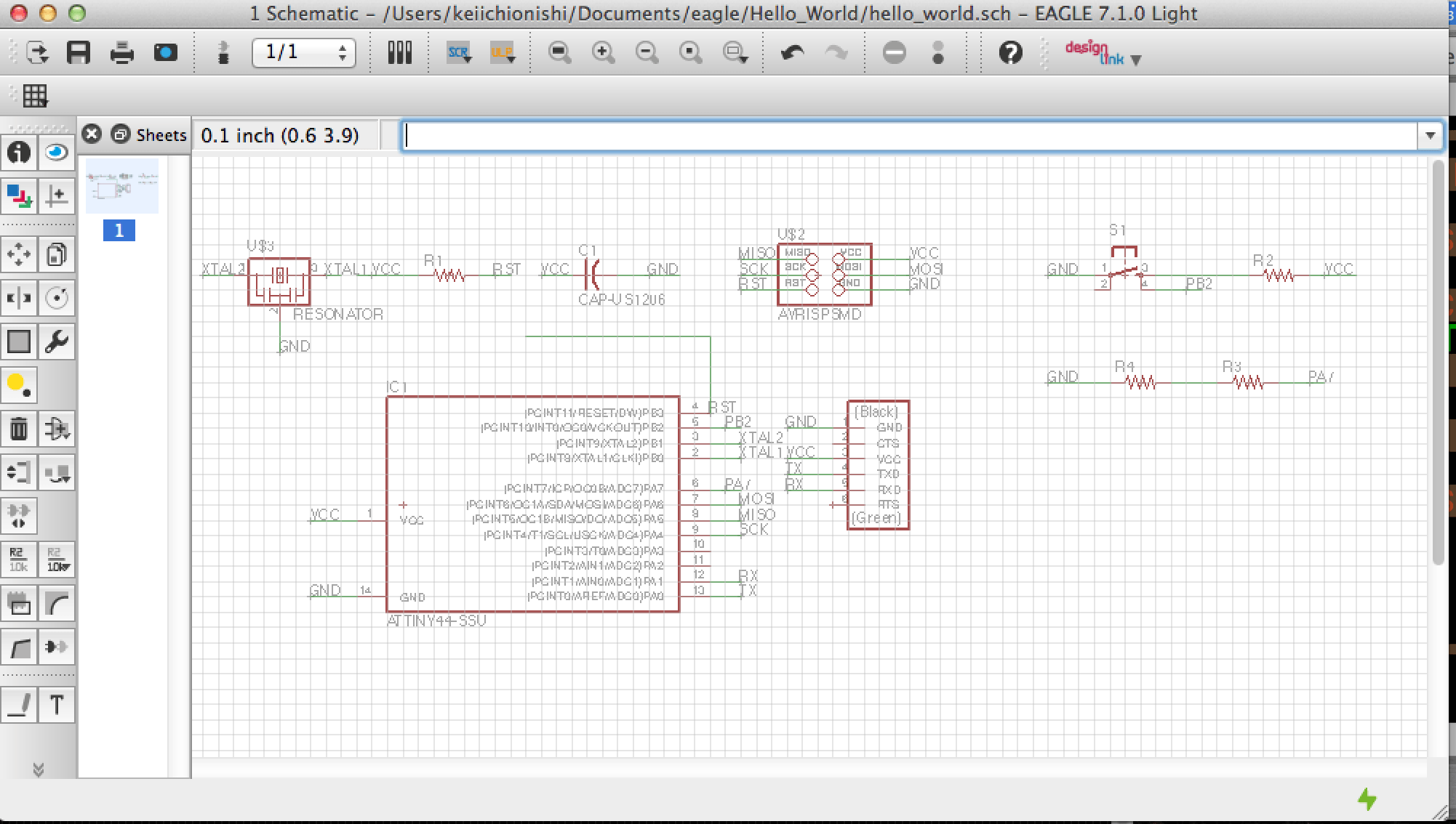
I opened fab library and picked components I needed and placed them on schematic work window. One thing I did was labeling each pins/wires and netting each others for every sinlge pieces right after I placed each components. Otherwise you would miss which component is for what. I also roughly arranged each components everytime I add new component not to mess up overall layout with tons of yellow wires. I also used 16 mil grid to understand clearance between each components and wires. 16 mil is diameter of milling cutter.
Step 3: Finalizing board layout
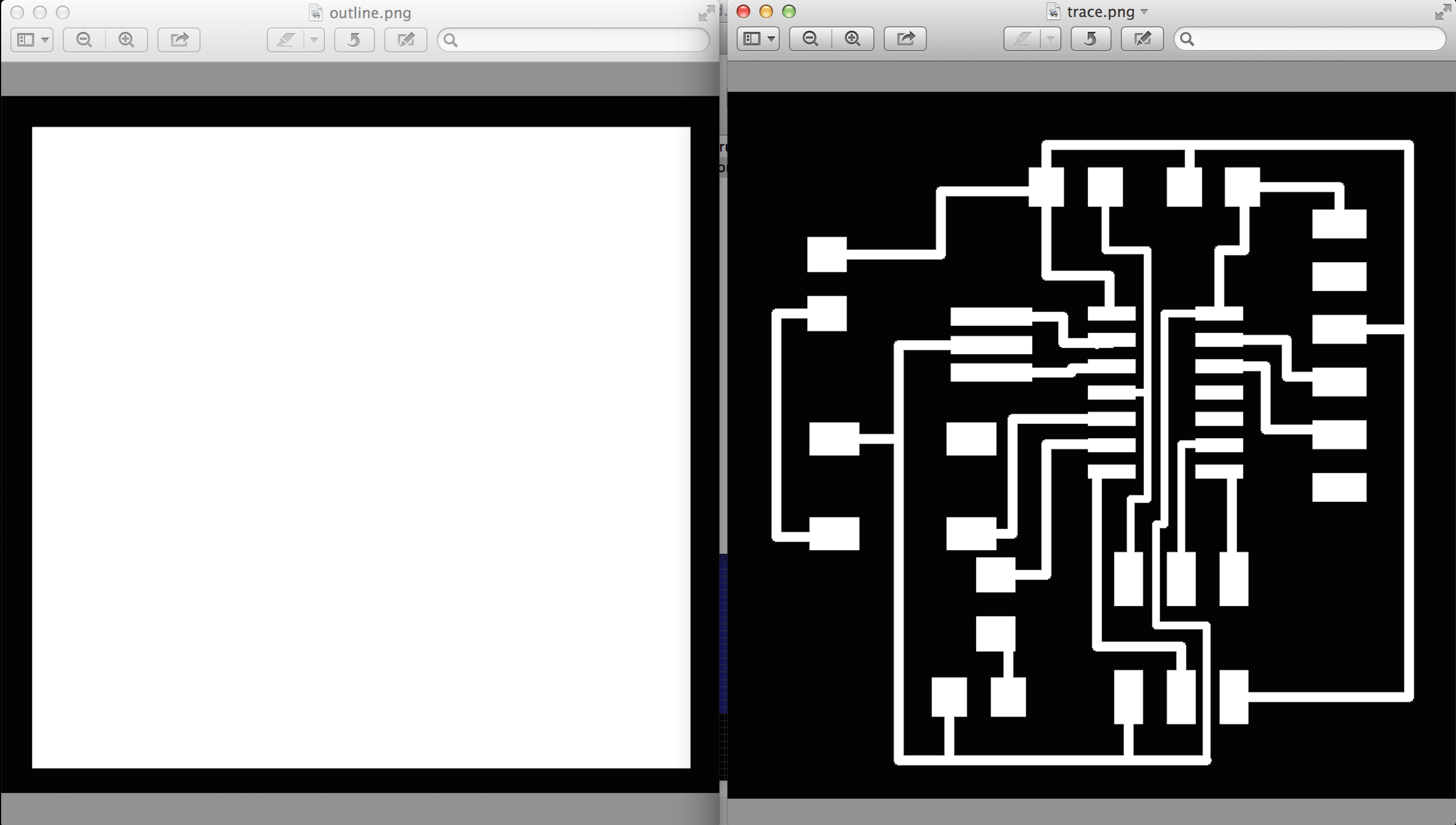
Once we have all components connected and placed on schematic, we can finalize layout of each components in board window. I wired each components making sure there is no electrical shortage. You can check the board using "fablab.dru" that can check whether the board follows design rules. You type "drc" command to use this function, and it found wire of 16 mil didn't work at some area assuring minimum 16 mil clearance between components and wires. I changed wire width from 16 to 12, and arranged layout manually. To make small adjustment, chaging grid size from 16 mil to 8 mil would help. Next step is placing a rectangle using different layer to determine outline area covering all trace area. Then, you define board size adjusting white rectangle. To export the design as an image, you go file>export>image. After setting 1)location to save png file, 2)monochrome, 3) Resolution at 500, you will get png image file. You need to export both trace and outline separately choosing one layer each.
Step 4: Fabricating PCB
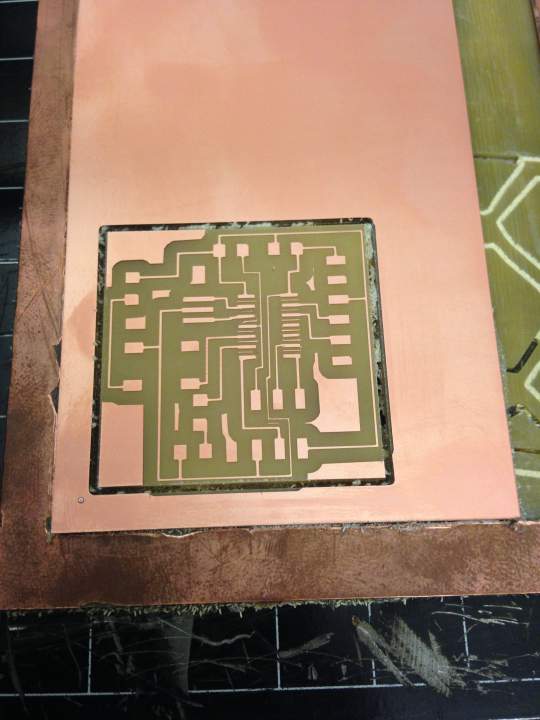
Like as we did 3 weeks ago, I cut out my board using Modela. Last time I used online version of fab module, but I used desktop version of that due to handshaking process between PC and Modela. Milling process went quite smoothly for both tracing and outlining. The only change I made on parameter setting was cutting depth for tracing. Default setting was -0.1mm, but I changed it to -0.15mm follwoing the person behind me. After the board came up, I realized wires between each footprints were thinner than I expected. I should have arranged each componets allowing minimum with of wires is 16 mil. Otherwise wires could be damaged during soldering process.
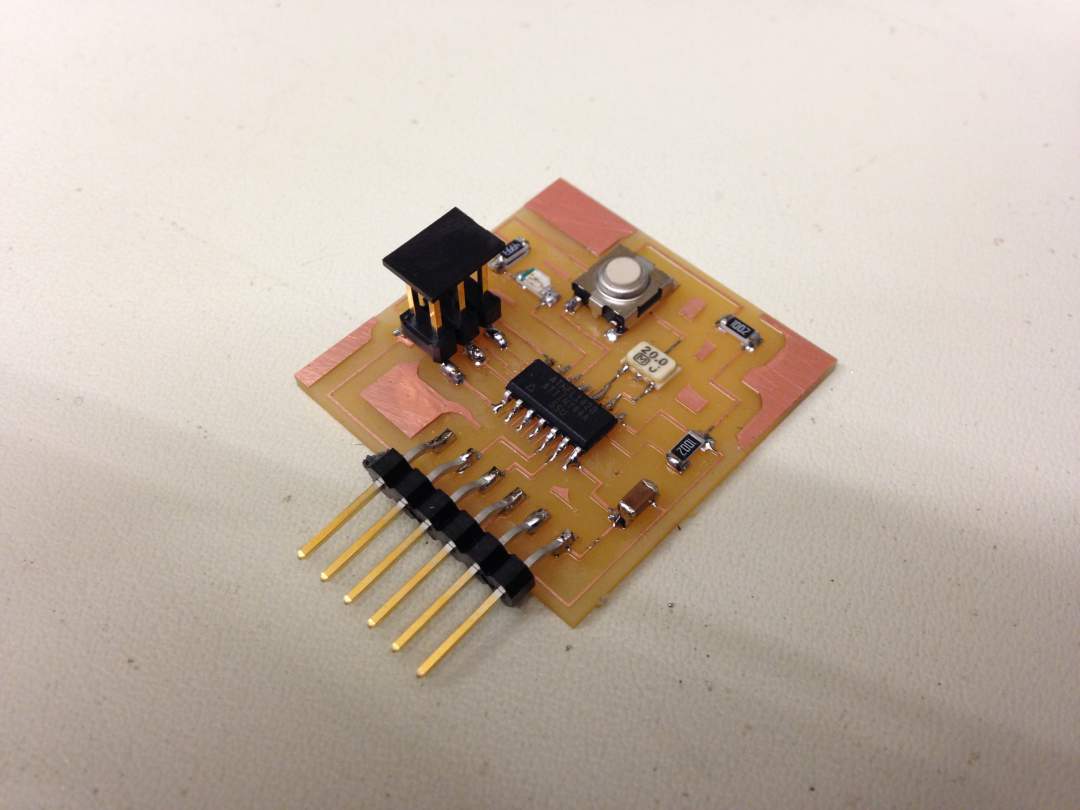
Step 5: Soldering
I used red LED with 250 ohm resistor other than default components. I put 10k ohm resistor for omron switch. Although the width of each wire was narrow, soldering process went well. I think I went through the learning curve of soldering technique. I will prgram it next week!