
Week Five: Electronics Design
LED current-limiting resistor choice: I want to use a blue LED (if we do in fact have those), and the range of forward voltages for the one we'd have in the class inventory, Digi-Key 160-1889-1-ND, is 2.8-3.8V. With a nominal supply voltage of 5V and 200 Ohms resistance (2x100 Ohm resistors in series because the only values we have are 100 and 499 Ohms) the LED will draw 6-12 mA (LED absolute max 20 mA).
To get started with Eagle I used Jeremy Blum's YouTube tutorials (well worth the time) and Sparkfun's written tutorials.
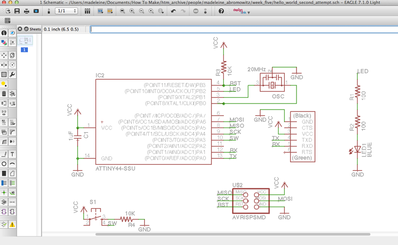
One thing Jean-François pointed out was that the pull-down resistor on the switch is unnecessary since we can use the internal pull-up instead. So if I were going to improve this board, I'd take that out.
The schematic was straightforward to put together, but the layout was harder until I took Palash's advice and started from Neil's example as a starting point. From there it was much easier to incorporate the switch and the LED and its resistors. But I wonder how I would have done it without a starting point, because whether or not it's even possible to route all the wires on one layer depends on how you assign pins. After two hours of trial and error I hadn't gotten anywhere, and this is a simple board, so there must be better strategies.
At one point I tried ripping up all the traces and using the Autorouter tool to see whether there was a solution at all, given my pin assignments. (You can confine the traces to the top layer as shown below.) It failed, so I tried again with a 1 mil grid thinking too large a grid might have been the problem, but it still failed. At this point I would have tried moving the switch/LED to different pins, but I ended up trying what Palash suggested first, and found a solution using all the same connections. So it looks like the Autorouter must not be guaranteed to find a solution even there is one.
While experimenting with layouts I didn't bother making the traces neat:
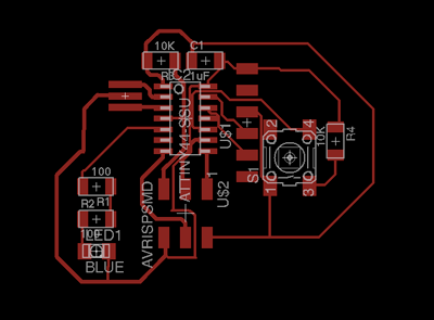
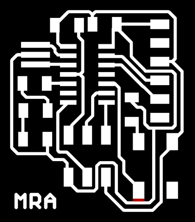
Here it is cleaned up:

The clearances between traces are 17 mils, and the traces are 16 mils wide.
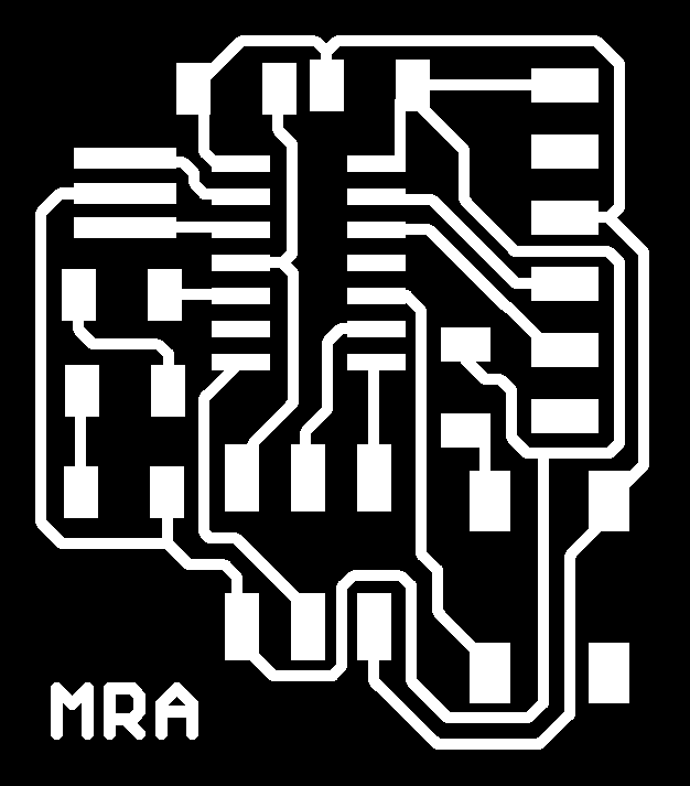
To get a black and white png from Eagle, make sure the right layers are showing, then File->Export->Image. Use 600 dpi, and check "monochrome."
I exported both the the Dimension layer (#20) with the outline and the Top and Pads layers (#1 and #17) with all the copper all at once and then split them into two images in Photoshop, but it might have been easier to do them one at a time.
My outline was originally 8 mils wide, but the fab module wouldn't calculate a path for a line thinner than the tool diameter, at least not around the edge of the image. So I widened the border in Photoshop to 1/32" = 19 pixels at 600 dpi, and that worked.
The images below are full size and can be used for milling.

Milling the board on the Modela (cut depth 0.2mm for the traces, settings otherwise defaults), this still resulted in one short between a pad and a trace, which I cut by hand.


If I were redoing this, I'd widen the gap between the pad and trace that were shorted together:
Here it is with components:
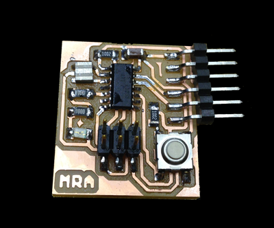
Sadly there were not actually any blue LEDs in the CBA electronics room. So I used a red one instead. With two spots for current-limiting resistors, my options were 200 Ohms, 250 Ohms (adding an extra wire to put two 499's in parallel), or 499 Ohms (499 + 0); I used 200, which with forward voltage 1.8-2.4 should put the current around 13-16 mA (LED absolute max 40 mA).