Message from the future:
Errors in this board were found when using it. VCC is not connect to the ATtiny, the capacitor is misplaced, it should just connect VCC to GND, and the SCK pin is also not connected here. A very good tutorial I found when fixing this is from the Fab Acacemy at AS220.
Circuit Design in Eagle
This week we all made programmer boards. In addition to the bare components we need to make a programmer board, which are the micro-controller (we used ATTINY44), a 20mHz crystal, a 2x3 pin header (for initially programming the board) and 6x1 output pins for serial communication. We had to add a LED and a switch as well. To design the board I used a free program called Eagle. Eagle has 3 main sections; the control panel, schematic view and board layout. Below is a snip of the control panel, which is where you can view all your libraries, design regulations and projects.
In the schematic view you see your board with all the components you'll need and labeled leads coming out to tell you what connects to what without having to deal with the rats nest of wires. To put a component in, type add and a window will pop up with components from your library. We had a "fab.lbr" which was downloaded from the course site and gets updated by the class, so check this page in the tutorials section of the class page for the latest version. To make a wire in the schematic view type "net" and draw your wire. Then create a label by typing "label" and clicking what you want to label. Be careful, label does not name the components, it just puts a tag there. After labeling you need to type "name" and go back and name each component individually. If you name things the same a pop up will appear warning you that components will be connected, this links them and carries the connection into the board layout.
To transition to the board view click the button I show here circled in red on the top of your panel. By pushing here you make sure the two views are synced, if you just minimize and open the other view that may not be the case. After creating a schematic and opening the board layout you'll have a the rats nest of overlapping wires.
To start laying out the parts on the board, move each component around and try to make as few overlaps in the yellow rats nest lines as possible. You can use resistors, capacitors, and other components to jump tracks. Some useful Eagle commands I used in the board window were route (which places tracks where you click), rat (which removes extra wires and reroutes the guide lines to the shortest path) and show VCC/GND/whatever component you type (which highlight whichever component you highlight).
After all the finicking to get the board to look how I wanted it I checked the design rules to see that it could actually be milled with the fab modules. To check this you have to download the fablab.dru file to the dru folder of your Eagle program files. Then you can go to the Edit tab of the board layout in Eagle and select Design Rules, run it and it will tell you if it is possible to mill your board. For example, it will say if traces are too close together to run the 1/64" bit between them. After this I added a background to the board layout to show where to cut out the board. You can insert a rectangle, or any other shape and edit it like I did to get a circular background. Move the white lines in around your components and background so you don't have so much extra space on your boards.
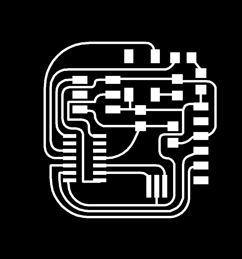
After finishing the design in Eagle you need to export PNGs in monochrome for the online fab module. You'll want one PNG for the traces and one for the outline and they must be at least 500 DPI. To show only the layers for each, go to View > Layer Settings and click "none" to deselect all. Then click just on "Top" which is the first layer shown and ok. Then only the traces will show. Do the same thing for the bottom layer to get the outline. Then File > Export > Image to get each PNG. To make sure the traces and the outline match up, do not move the white lines which depict the working board between exporting the images (I made this mistake...) Here's what my final board looks like, the traces and the outline. Each was then fed into the fab modules per usual, found at mod.cba.mit.edu/ To get the fab module to work on the west section Modela mini mill you have to load the settings saved to the desktop and the modules server must also be running.


Milling & Stuffing
My first two attempts I made at cutting the circuit board failed. The first time the Modela didn't play well with the fab module and when I tried to cut out the outline the mill just cut diagonally through my board. I was pretty surprised and confused by this, because the paths the module laid out looked fine, there's a screen shot below.
I cut the rest of the cut board out on the shear paper cutter, which was pretty nifty. I tried to solder over the cut traces to salvage the board, but it wasn't very successful. Attempt 2 failed because I cut the board to shallow. As you can see below the outline of the traces are shiny because there is still copper there. I could have re-zeroed and re-run the mill, but I needed to go to class.
Attempt 3 was a success! I came back to the Modela and she worked perfectly with time and played well with the fab modules.
Then onto stuffing the board. I was much better yielding the soldering iron and tweezers this time around with a little bit of experience. I did have a hard time telling which size resistors to use though... I looked through a lot of other peoples blogs and the values seemed all over the place, so I chose 2 x 10kOhm resistors and one 500 Ohm resistor for the current limiting resistor from the LED.