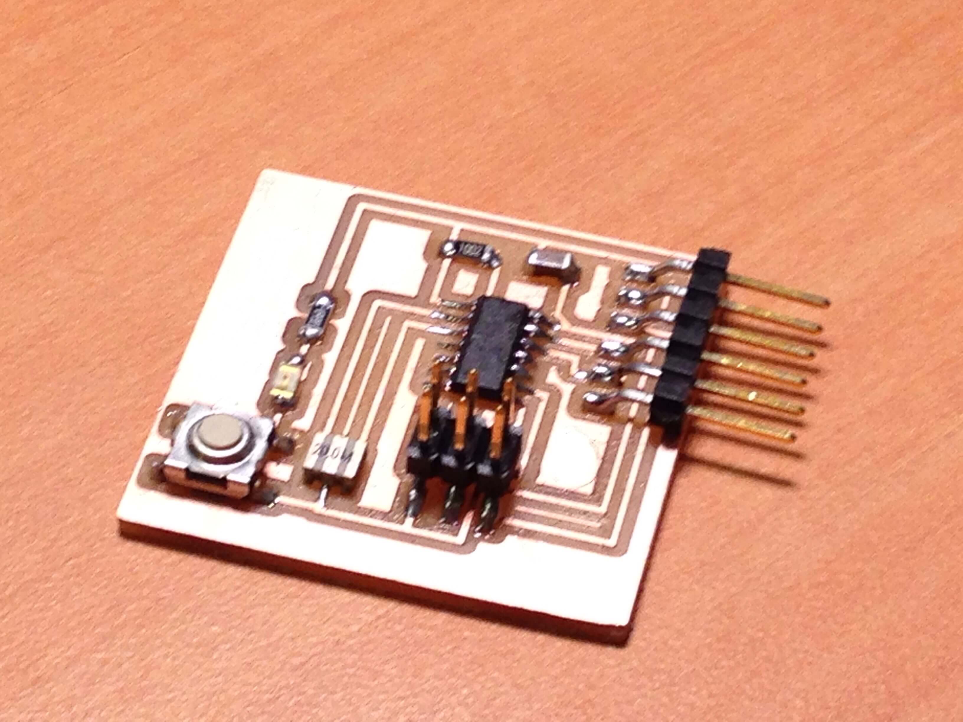
Designing
This week’s prompt was straight forward. I had some experience with building electronics, but not design. I decided to use Eagle because that was the program presented in recitation.
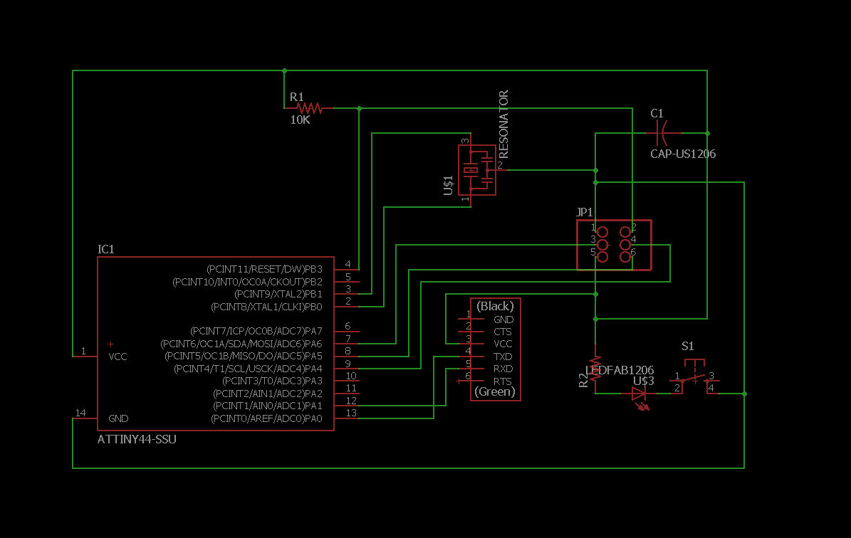
Schematic
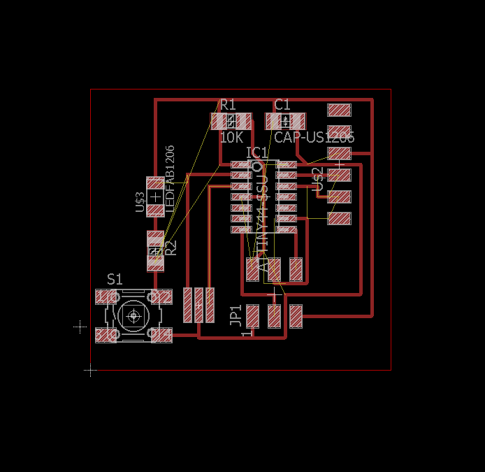
Board
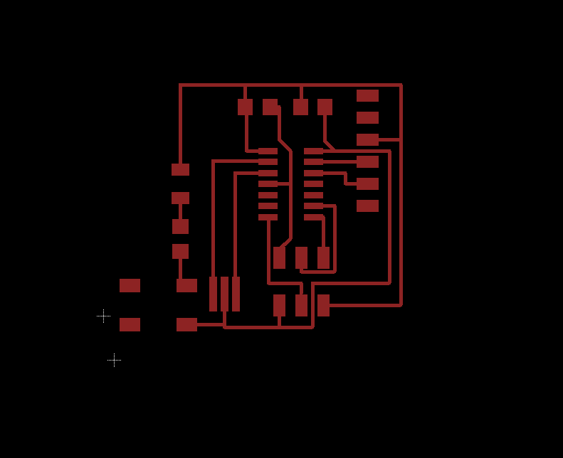
Layout
Modeling
I know the TAs showed us a way to export the border directly from Eagle, but for the life of me I couldn’t remember how to do it. So I put the design into paint, slightly increased the size of the paper and then eyeballed then selected and centered the circuit by eyeballing it. I saved here in case I made a mistake. Then I filled in the border and exported that for my trace cut. Then I opened the original file and painted in the traces.
Definitely had some failures with the boarder before I got that little trick worked out:
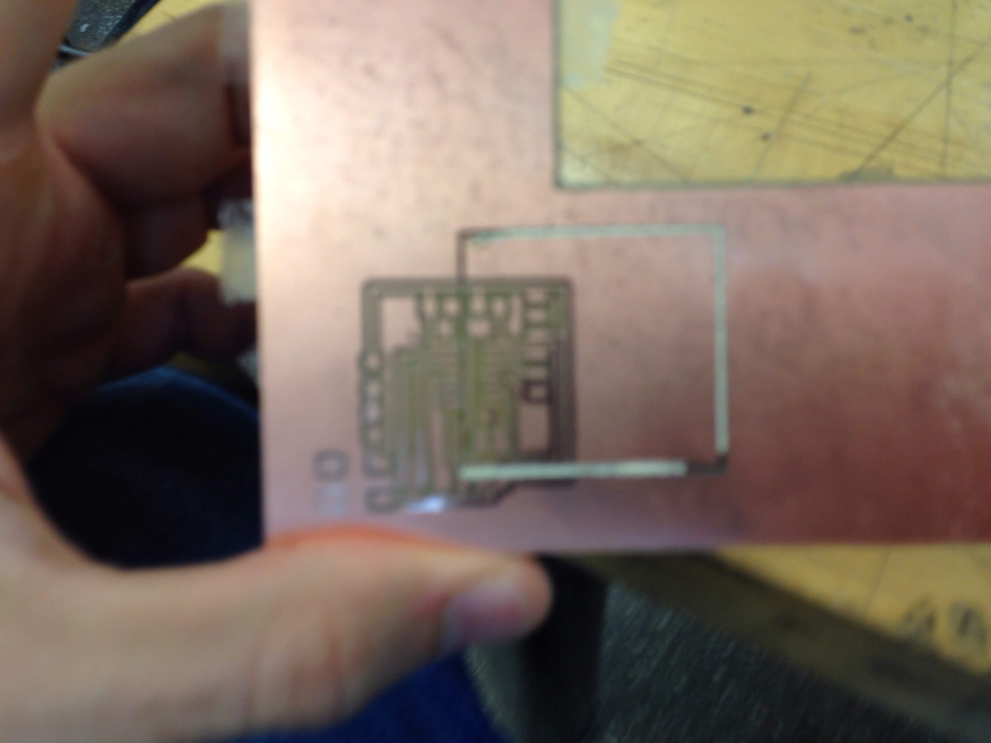
First failure . . . of many
Word to the wise: the first time I did this I copied the circuit into a new paint file. When I went to turn on the mill, it started to cut out my circuit on a much, much larger scale than I intended. For those of us without that much experience with image processing, the reason was when I opened the new file it automatically selected the “canvas” size to be about 7X7 inches. The original export from Eagle was the correct size of about 1X1.5 inches. You manually increase the border edges by dragging the arrow horizontally or vertically from the sides of the image in paint. You cannot, as I discovered, drag the diagonal because it increases the size of the image itself and not the canvas. Complexities!
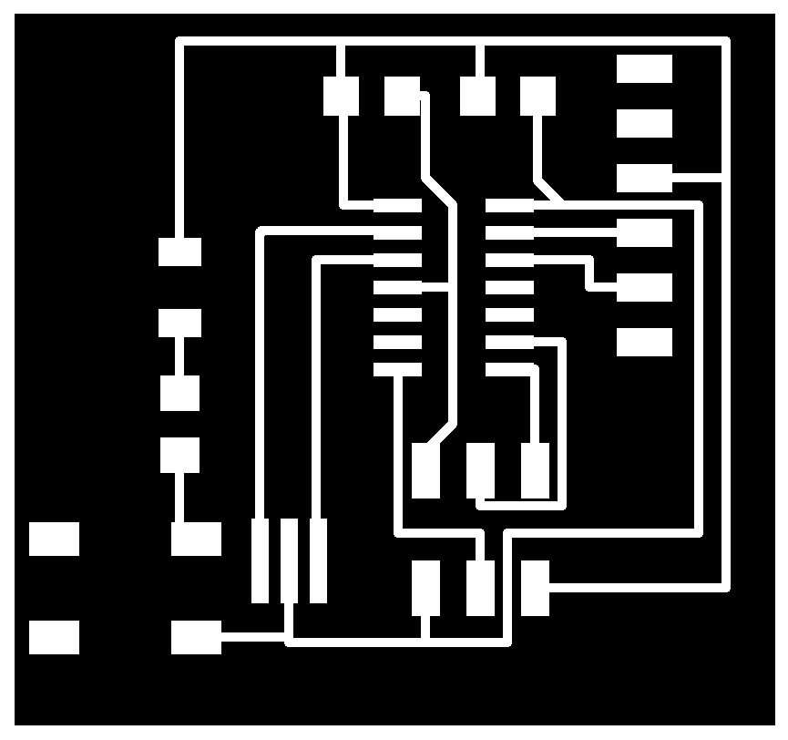
Final PNG
Making
There was a ton of excess material lying around the mill. So I did my best to use stock that had already been cut.
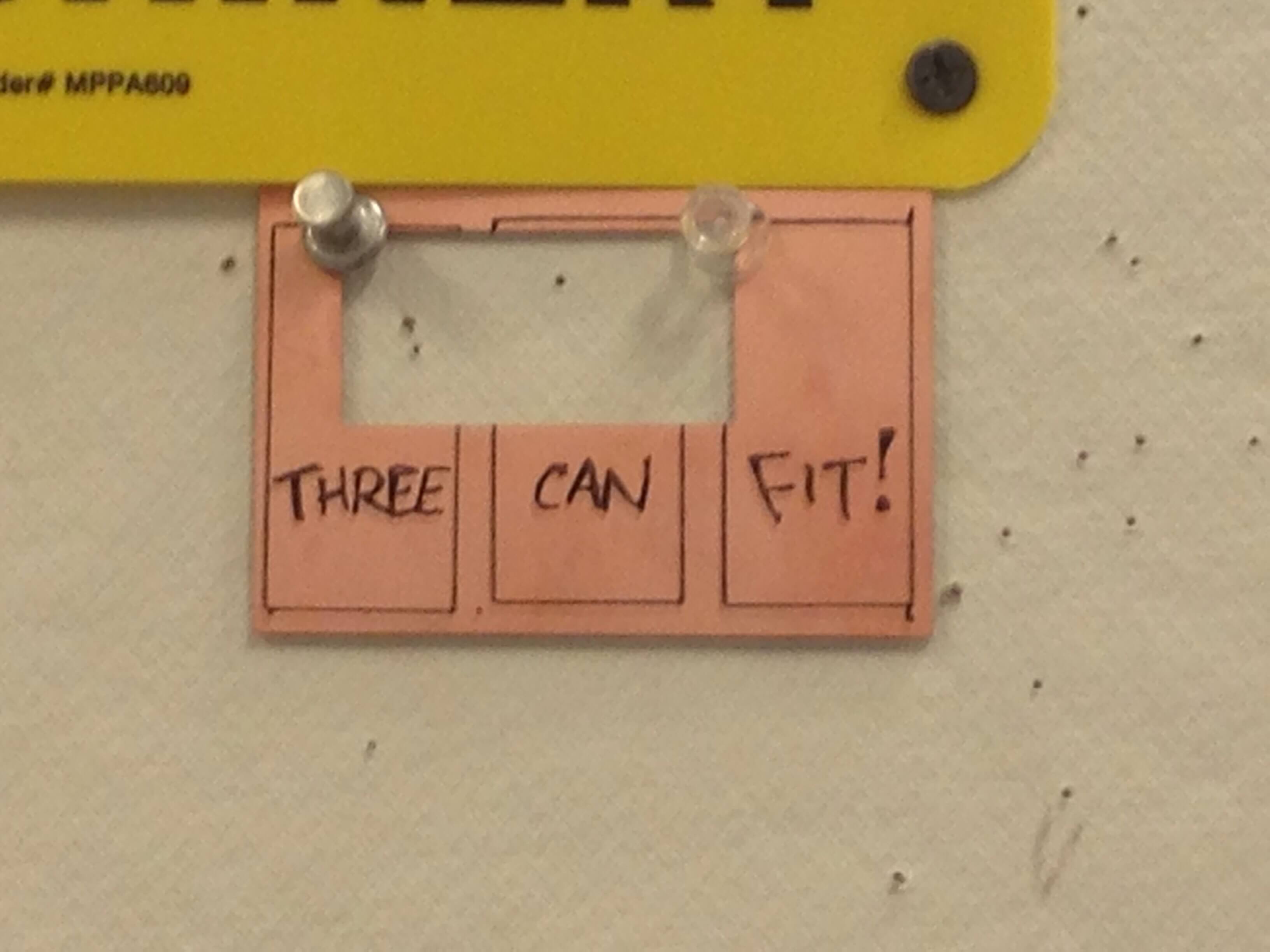
Indeed . . .
I think the mill platform needed to be leveled because I was having serious issues with a change in the depth of cut over the area of the board. I also struggled with adhering the board to the sacrificial layer. This might indicate that the sacrificial layer needed to be replaced. I resolved this issue by setting the cut depth low (.3mm rather than .1mm) and moving the board to the upper right of the platform, where there it was flatter.
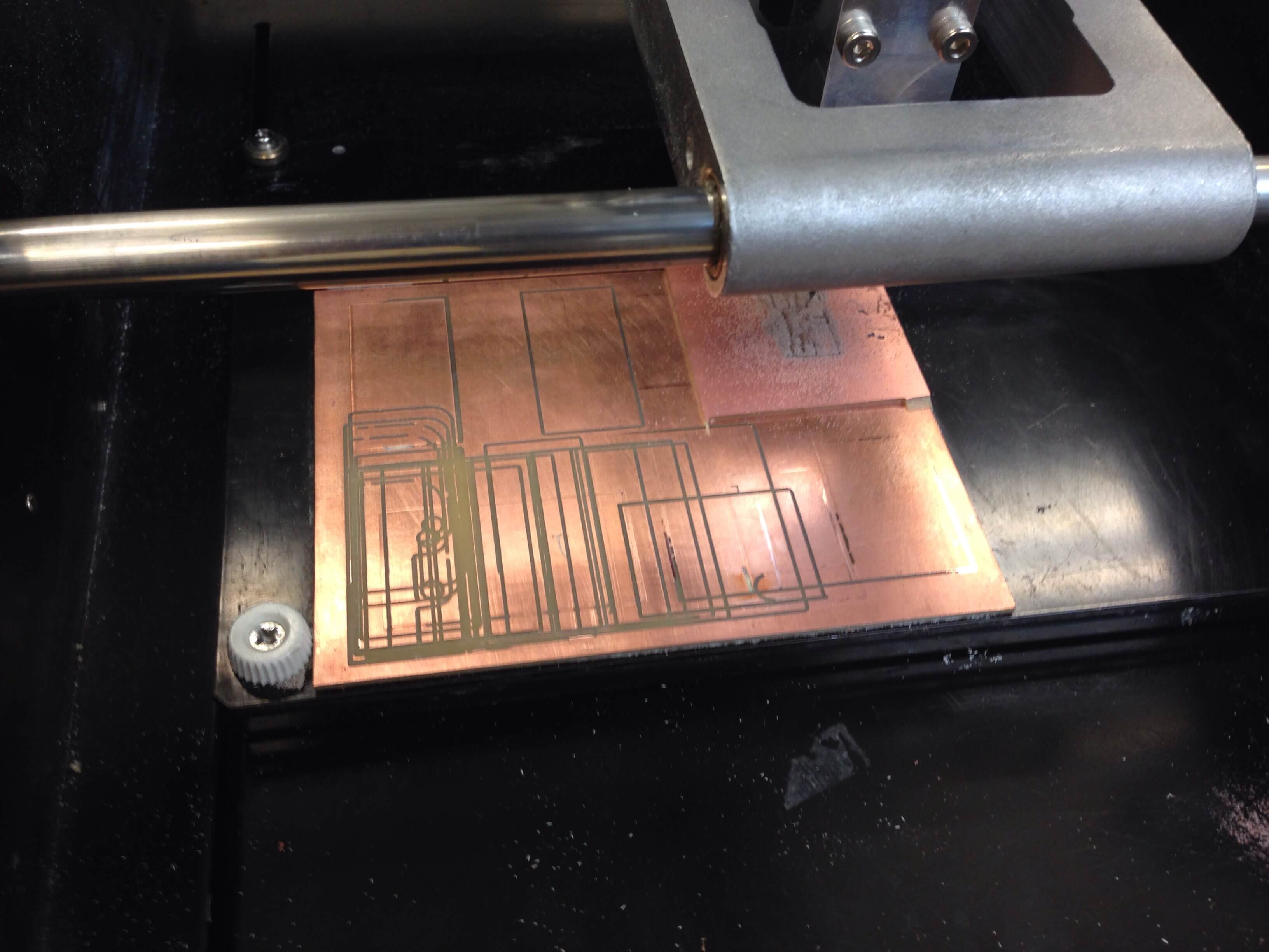
An effective way to solve depth issues
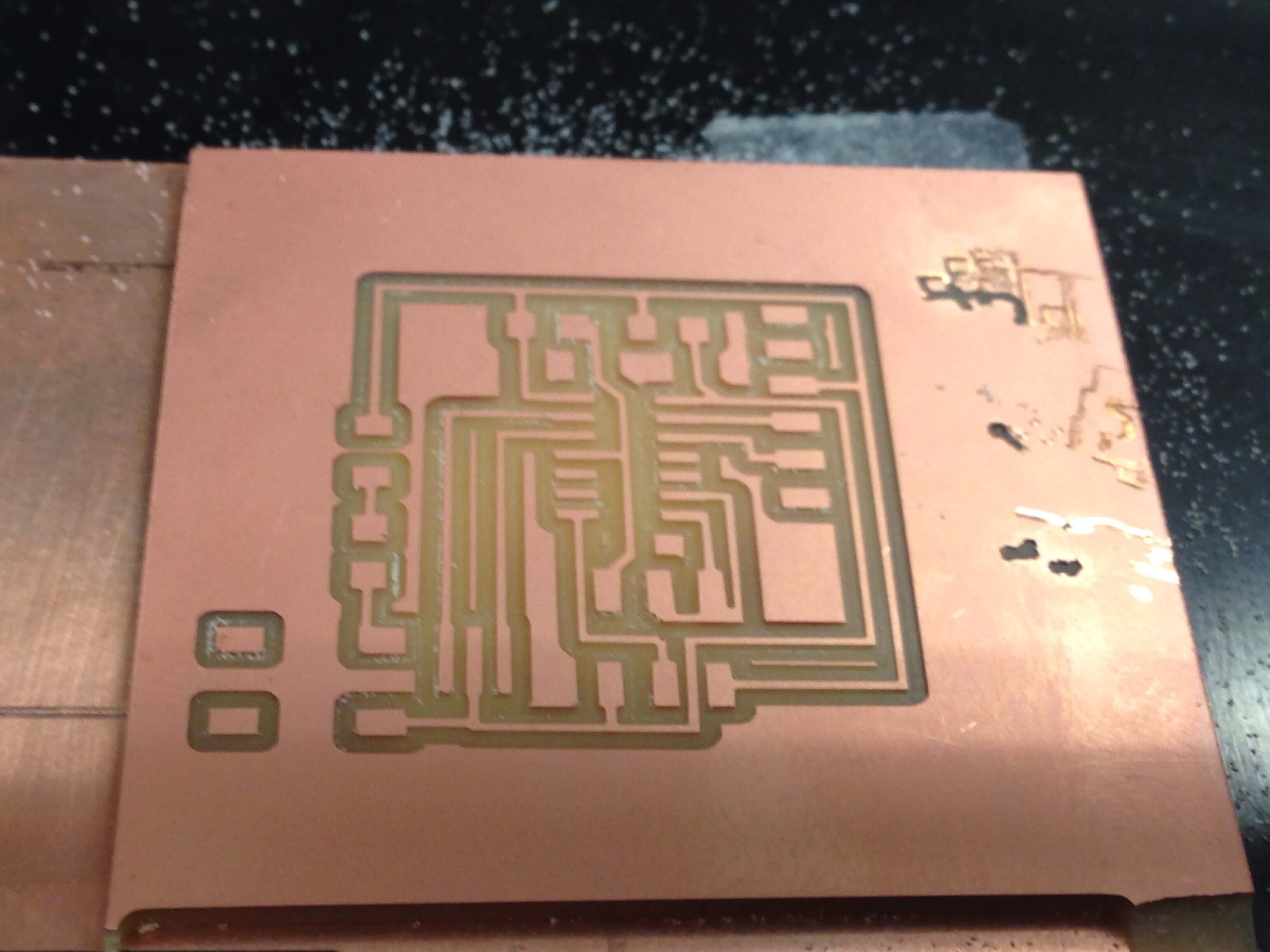
Final board
There’s a subtle problem here that I’m not sure how to avoid. If you look again at the picture above:

An issue
A pin and a trace had not been separated by the mill, which is a problem I would have found had I looked at the fab modules before cutting:
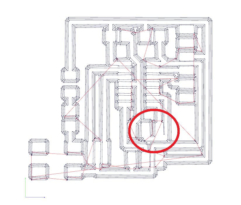
Paying attention here would have helped
The root cause of this failure is the grid setting in eagle, something that can be changed with this button:
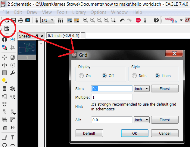
Root cause of the issue
This lowers the constraints on where you can run traces and would have allowed me to center that trace between the two pins.
Fortunately, I come from a profession that specializes in quick and dirty fixes. I took a razor to the board and completed the final cut myself. After the cut and installing the component, I applied a voltmeter to make sure that there was no connectivity between the traces.
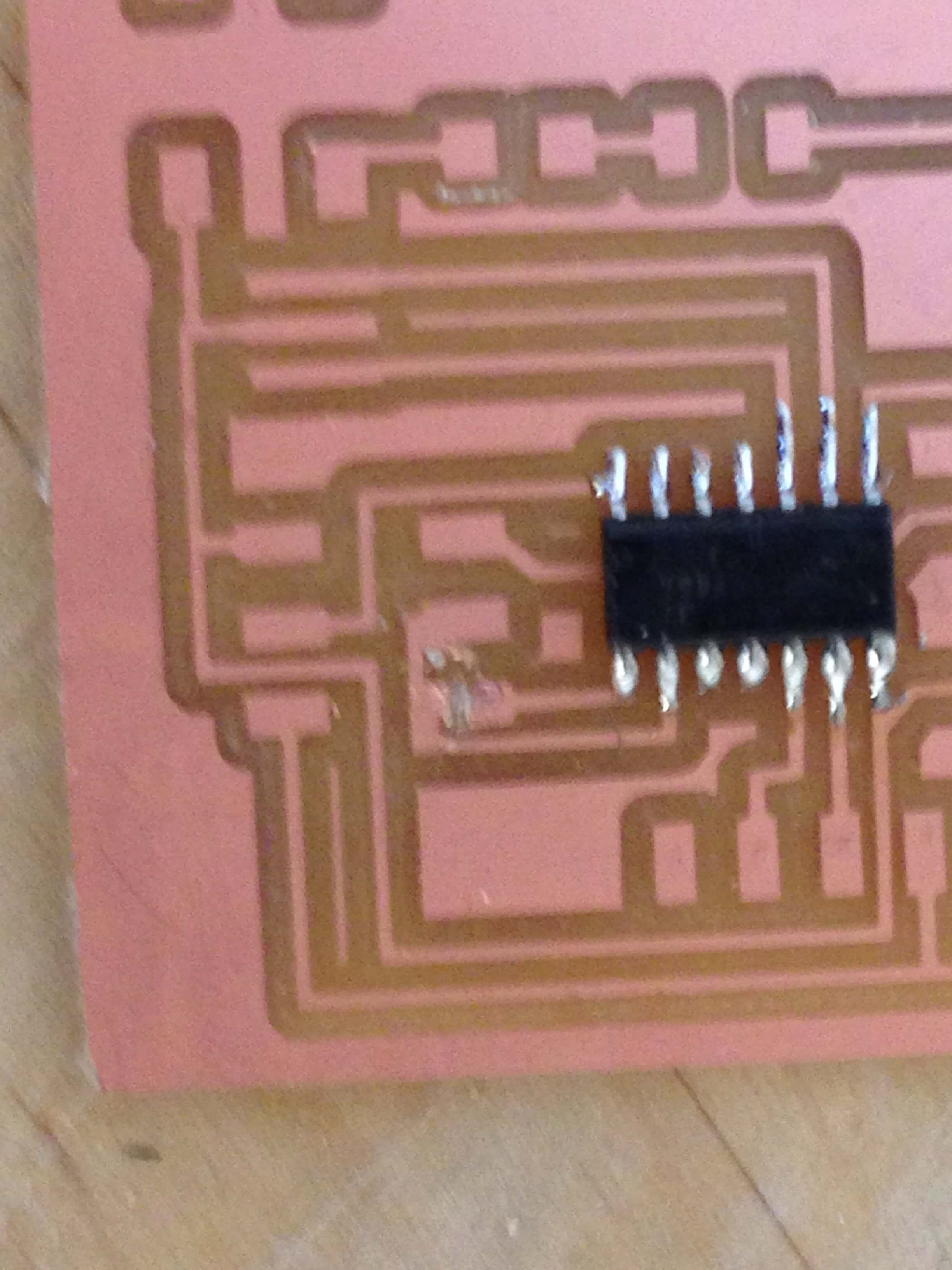
Nothing that cant be fixed with a razor and elbow grease
The rest of the installation went well and the board came out pretty. I’m just not sure if it works.
