Week 5: Electronics Design
Hello World!
October 19, 2015
Our task this week was to redraw the Hello World board and add (at least) a button and an LED. Life has been particularly hectic with Member's Week impending, so I decided to keep my scope small. As I mentioned during the Electronics Production week, I never learned how to use Eagle or design/ produce PCBs in college, despite being an EECS major, so I also wanted to give myself time to climb a potential Eagle learning curve... I started my Eagle foray with several Sparkfun tutorials that had been mentioned by students in previous years, as well as the Electronics Design tutorial from the fab pages. Here are links to the Sparkfun tutorials and some commentary:
- How to Install and Setup EAGLE: I didn't download the Sparkfun libraries, but this tutorial helped me see how and where to enable the fab.lbr file in the Control Panel > Libraries section. I also added the fab.dru file to the Control Panel > Design Rules section. Both of these files are linked in the Electronics Design tutorial.
- Using EAGLE: Schematic
- Using EAGLE: Board Layout
EAGLE tips, tricks and general usage, culled from reading the pages of students in previous years, the Sparkfun tutorials, and my own mistakes and questions:
- Instead of using buttons, you can use the "command line" interface in EAGLE, and type/ enter commands such as "add", "rotate", move"
- Save often, especially if your laptop is known to periodically crash :0
- Use ESC to get out of commands (like the add command, when you only want to add one component)
- Use "net" instead of "wire"
- Instead of wiring up everything in the schematic view, use the "name" command to give names to nets, and then use "label" to show those names. Then, when two nets have the same name, Eagle will know they are connected
- Use the "show" command to make sure that the correct pins are connected, even if they are only connected in name (instead of explicitly with a net)
- Changing grid size using "grid" can make routing tricky paths easier
- Airwires in the board view go to the center of each pad - make sure you bring your route to the center of the pad to ensure the Ratsnest is all cleaned up. You can also view the remaining "Unrouted" routes by displaying only these traces using the Display window/ command.
- Show, move and rotate are useful commands in both the Schematic view and the Board view
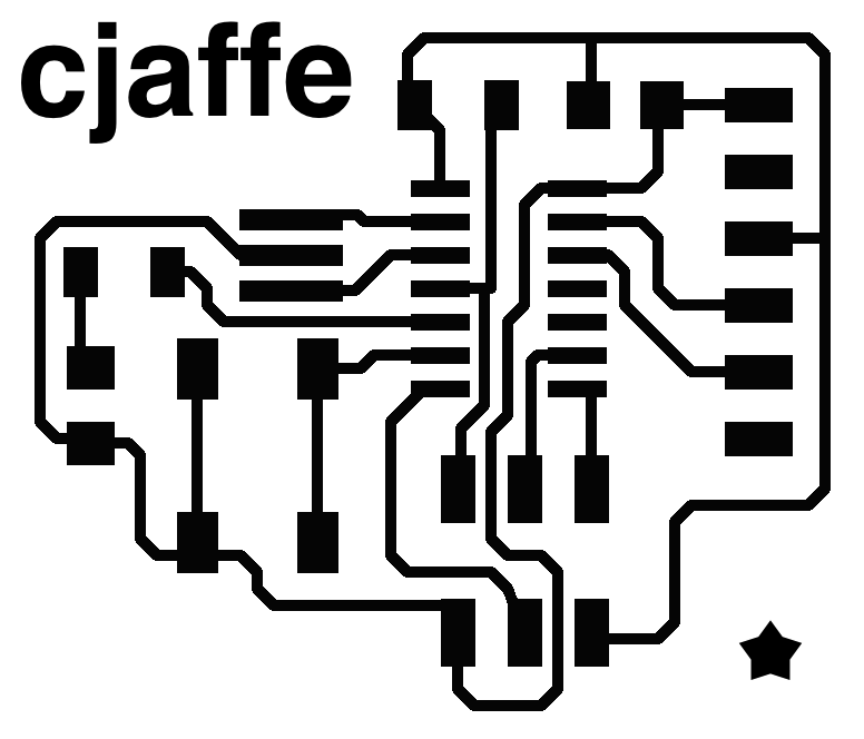
After a bit of playing around with Eagle schematics (and at least one do-over when my computer crashed), I came up with the following schematic. Definitely not gorgeous, but I feel like I am now reasonably comfortable with the basic operations in Eagle for schematics. I am planning to add a single switch/ button and an LED. I plan to program the board so that the button can change the blinking mode of the LED. Thanks to Jonathan Bobrow for answering my late-night Eagle questions. Now to lay out that board...

I soon realized why board routing was causing people so much trouble. Routing is clearly a non-trivial task, and I can imagine that anything much more complex than this board would be very difficult to route by hand. I spent a little time just getting comfortable with the board view, by laying down and ripping up a few routes. I decided to start out by trying to route the board like the original Hello World board. I used a route that allowed you to make 45 degree corners (I think I read on someone's page that "rounded" corners like this can give the circuit better electrical properties). By following the layout of the original board and adding my LED, pullup resistor and button on the bottom left of the board, I was able to get a pretty good layout without needing any jumper cables. I used the "Ratsnest" command to check my circuit, finding at first that a number of airwires within the pads were not connected. I fixed these and then used the fab.dru design rules to check my board. Unsurprisingly, the clearance between my traces underneath the IC were too close, as you can see below.


I decreased the grid size to 0.001 so that I could draw finer routes. After ~7 iterations of drawing routes, checking design rules, and moving my traces, I finally had a board that passed the design rules. I drew an outline around the traces using the "wire" command (this turned out to be not quite the right way to do it, more on this later). Then, I used the "display" command to selectively display and export the different layers. I exported the traces and the board outline separately, at 600 dpi each. I added my name and a star manually, and figured I could invert the image in fabmodules.


Next up: milling and stuffing the board. Should be easy, right? Not quite. (By now, readers can expect this as a recurring motif). To start, I had to mill a few iterations of the board. I milled the traces using the same settings as last time (.12 mm cut depth, 5 offsets), and they came out beautifully. My troubles arose when I tried to cut out the board. I realized (after consulting with John), that the board outline I had created in Eagle was too skinny for the 1/32 endmill. I used Paint to make the border wider, but when I went to mill the outline, disaster struck! When I loaded the new png, I did not set the dpi appropriately, so the scale was completely off, and the mill cut right through my traces. Disappointing, but not insurmountable. (By the way, I used the default settings in fab modules for the 1/32 endmill). I still had space on the PCB stock, so I repositioned it, and milled my traces again. This time, before milling the outline, I made sure to set the dpi to 600 and checked that the dimensions looked approximately correct. Unfortunately, this outline cut was not perfect either, and some of my traces were clipped. I think this happened because I thickened the board outline, which pushed the internal edge of the cut up towards the traces. However, this mistake is still a little unclear to me. I don't feel like I know how to set the origin point in fab modules so I feel a little shaky on this skill. Luckily, all my pads were intact, so I decided to proceed with the slightly clipped board and use wires to patch the clipped routes.


Next, I went to the basement lab to stuff the board. The wires were a little tricky to maneuver, but overall, soldering and stuffing went pretty smoothly. I used more flux than last time and tried to heat both the pads and the component "feet", which made the surface mount soldering go much more smoothly. I also made ample use of the microscope to make sure my components connections were smooth. The only wrinkle in this part of the process is that, after I had finished stuffing the board, I discovered that three of four of the pins on the ATTiny44 were shorted. Frustrating! I couldn't see any debris between them on the board, so I ended up removing the ATTiny, and discovered that the traces actually shorted these pins under the board. I hadn't noticed it after milling, but I guess the clearance between the traces was not big enough after all, despite having passed the design rules check. (I later learned that the design rules file had been updated so I suppose I was using an outdated version.) I used an Exacto knife to separate the traces, and resoldered the ATTiny for a "finished product" with no incorrect shorts. Now to attempt to program the board...


As suggested by Amanda and Dan (whose pages were very helpful), I followed the High Low Tech tutorial to be able to use Arduino software to program my new board using the FabISP from Week 2. I hooked the FabISP up to my computer with a mini-USB cable, the Hello World board to my computer with an FTDI-USB cable, and the FabISP to the Hello World board with the ISP header cable. Even after following the tutorial, things did not go smoothly immediately. Miguel helped me use the multimeter to debug two important issues: (1) I had soldered my LED on backwards and (2) I used the wrong pin number in my code. I thought the pin numbering went by the number on the inside of the IC in the diagram below, but the numbering actually uses the numbers on the outside. My LED is hooked up to Pin 8 (the PWM pin on the left side of the IC), but I had been using "5" in my code.

After these fixes, I incrementally increased the complexity of my program to first just turn the LED on, then turn the LED on when the button was pushed, and then to switch between fast and slow blinking depending on whether or not the button is pushed. I wanted to implement a "button mode" where pushes of the button changed the pattern of light blinking, but found that implementing state in the ATTiny was going to be too complicated given time constraints. I assume we'll get to that in the coming weeks :) It was pretty awesome to design and build a functional board from scratch and to program it using my own FabISP. Thanks to John Bobrow, Kim, Mike, Miguel, Andy, and Saquib for moral support/ debugging help/ equipment!


Design Files
- board-wk5.png (don't use - border too skinny!)
- traces-wk5.png