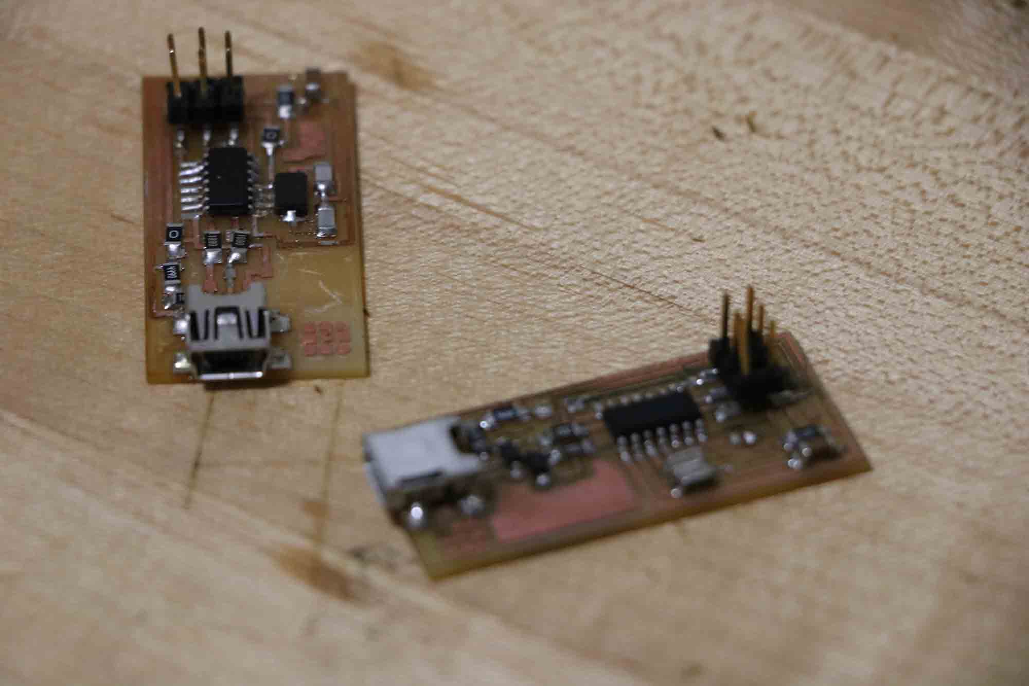
This post deserves a more appropriate title — How to manufacture a brand new PCB in less than 4 hours! That’s right! I set out with nothing but a schematic of a FabISP (in-system programmer for AVR microcontrollers) and had a functioning PCB only a few hours later, one that could act as programmer to program other boards. So meta!
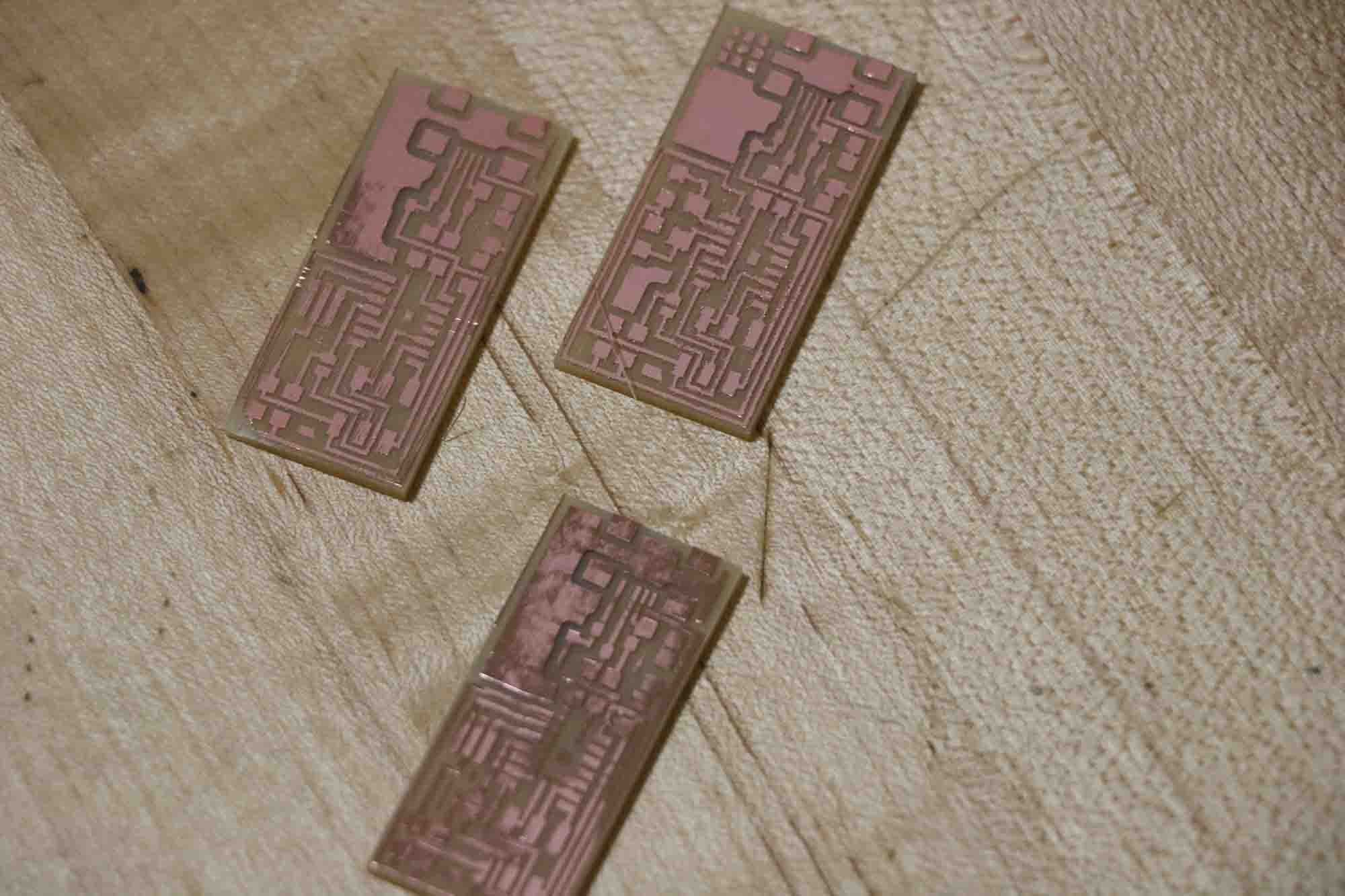
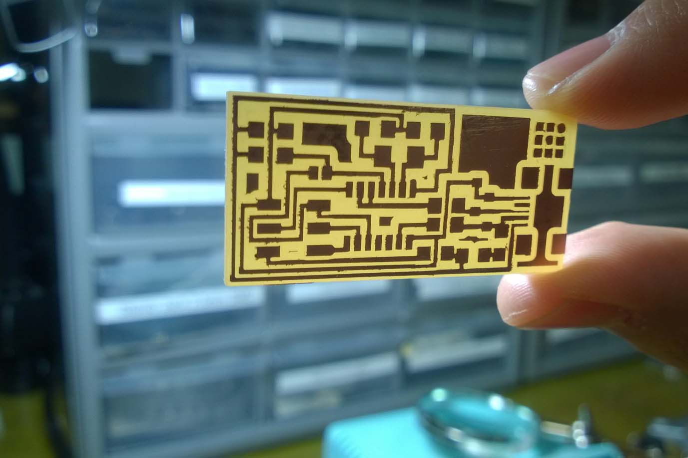
The FabISP board that we actually make here uses some ready compoents such as ATTiny44. This uC IC and others are laid out on a board that has copper substrate as the top layer. Instead of etching the schematic paths (as is normally done in the case of large volume), we use a milling technique here instead that mills out copper from the substrate to leave with copper pads and connection paths. The milling was performed in this case with the Roland Modela 2 (MDX-20) that has milling accuracy going upto 0.001 inches. In our case, however, the traces were fine to be cut out with a 1/64 inch endmill (and the outer board boundary with a 1/32 inch endmill).
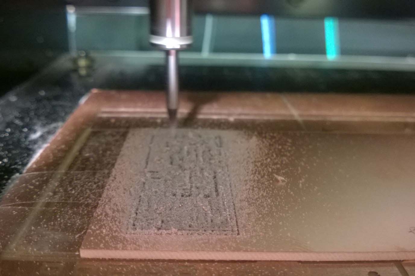 You start by putting the board on a sacrificial layer in a way that it doesn't move when there's contact of the endmill with the board and the traces are being cut. The endmill is then moved into the right x, y coordinates using the FabModules and with the appropriate parameters set for your job (for my particular board: normal depth: 0.12mm, offset: 4 (can be increased to mill as much copper on board), speed: 4 (with a new endmill installed)), you start the milling process.
Things to take care of:
1. Use the double tape to paste the board on the sacrificial tightly so that it doeesn't move when the job is in progress or else it is going to leave marks and the process may even have to be restarted.
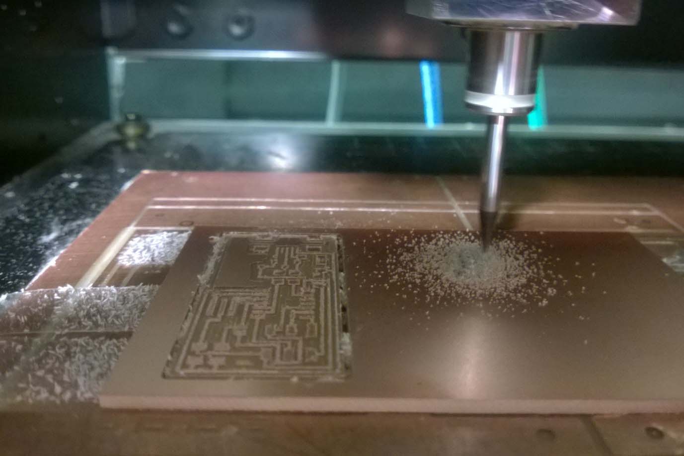 2. The first time I milled the board, I brought the endmill manually down to a much lower height leaving no space for it adjust its depth when move down for subsequent cuts in the process. As a result, the depth of the board being cut for the traces and the outside boundary turned out to be a bit shallow and the board didn't really get separated from the bigger PCB sheet.
3. The parameters of speed and depth need to be adjusted as per the condition of the endmill as well. If the endmill has worn out, it'd perhaps be better to run the milling at a lower speed (3 instead of 4 in FabModules).
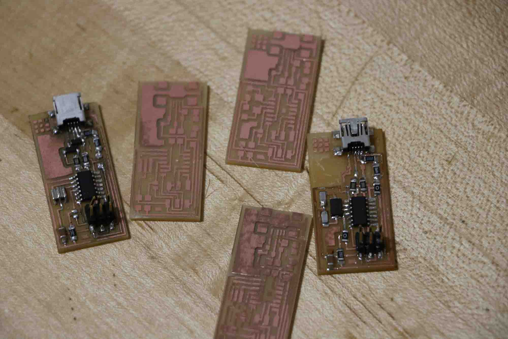
I cut out two small schematic patterns from a single sheet (although you could do three as well by careful adjustment of x, y from the beginning). I left the offset as 4 for this job, since it wasn't going to be a high frequency application where stray RF could affect the output in the circuit.
 Once finished with this process, it is important to scrape the board with a razor or a steel ruler to remove the copper left that could cause shorts and even problems during soldering. A perfectly smooth surface of the PCB can then be washed under the water as well. A smooth surface will help ensure solder sticks to the surface, doesn't create shorts and makes the board look cleaner as well. The parts need to be soldered on the board via surface mount and that's how tiny they actually are.
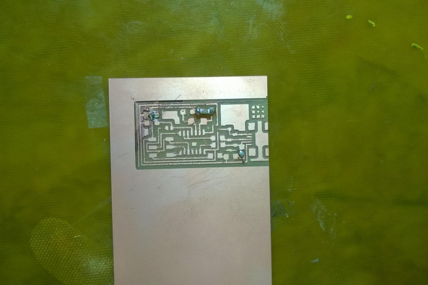 I went for soldering in the lab and realised that the tip of the iron was oxidized, so much so that the idea of the components with close legs (such as ATTiny, USB connector, ISP header) had to be ruled out. It didn't seem like the solder could be fixed by applying a lot of flux or by tinning it as well and I wasn't sure about where I was going to get new tips. I got the solder paste, however and applied the same on the board with plunger and then let the magic happen with the glue gun to fix the parts in place.
 This was the first time I was using this technique, for that matter, the first time doing the surface mounts and did some shorts which I had to remove using the iron and copper braid (especially in the UCB connector legs). After having fixed the parts in place, I checked for continuity again through all the parts and didn't get any visible or invisible.
For powering on the board, I used the micro USB and the IDC cable to connect with a previously built programmer (ISP 6-pin to ISP 6-pin) in the
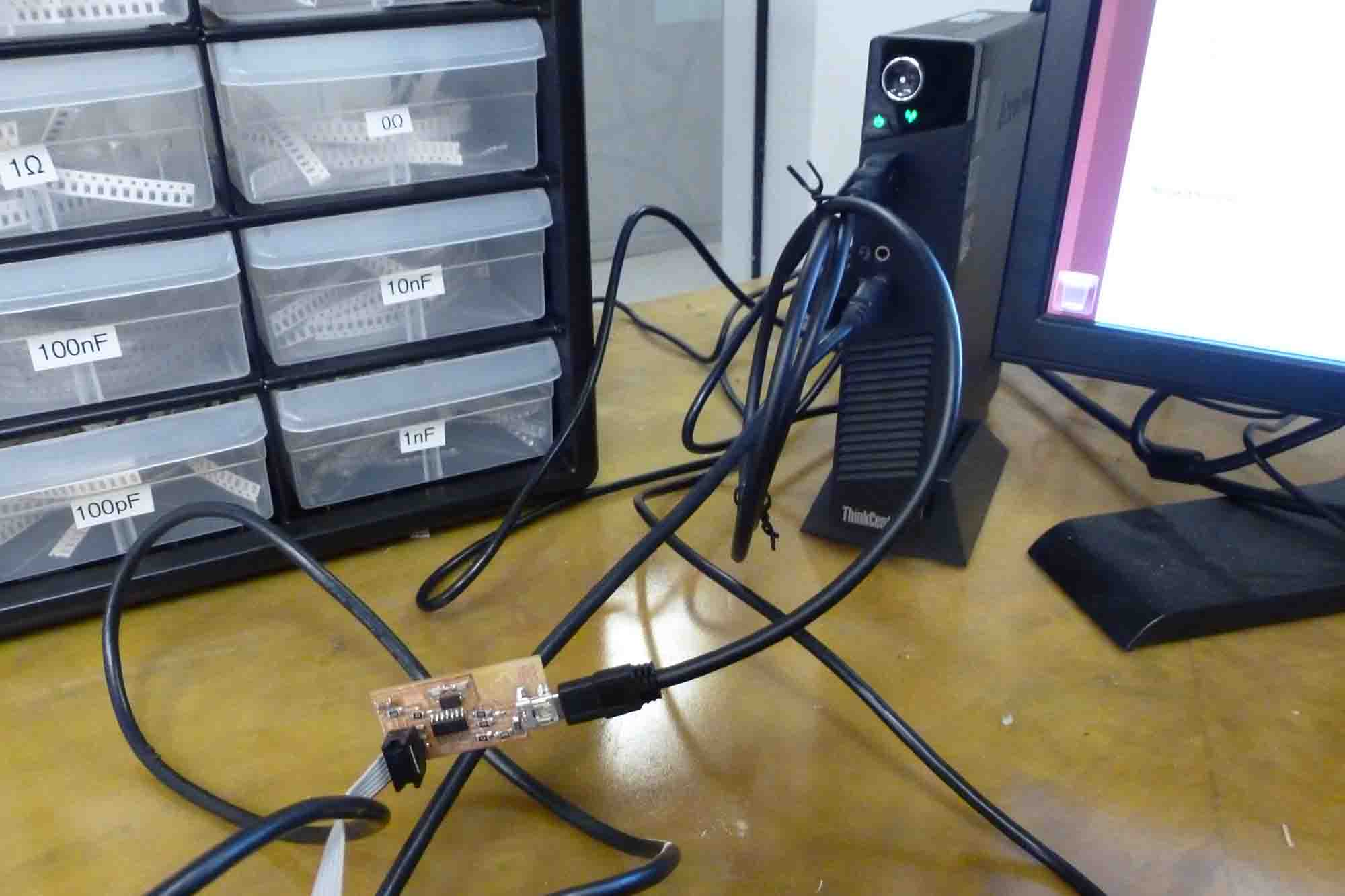 lab by Will. This programmer was going to help write the program on my newly fabricated PCB chip, for which I went to the terminal and carried out the following commands (while being in the firmware directory of the board and hvaing also installed AvrDude previously).
 make clean
make hex
(sudo) make fuse
(sudo) make program
And that's it! This is what the screen showed me, with the message at the end saying - 'AvrDude. Thank you!'
And voila, you have a functioning PCB that can act as a programmer itself, once you remove the two jumpers.
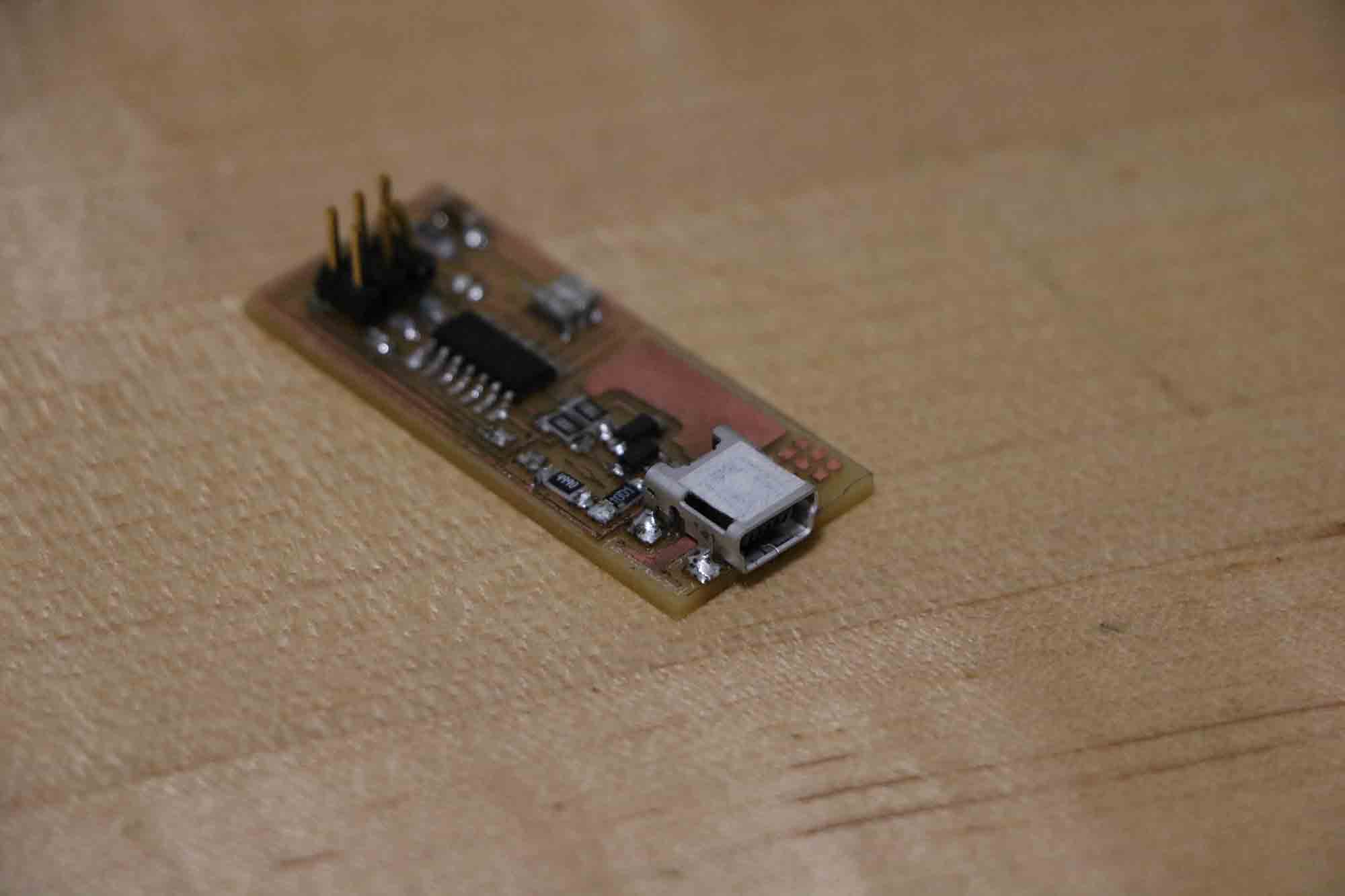 Following this, I went back and used the other traces file to mill the other board and came back to do usrface mounts this time with the soldering iron. And with the same process, I had another working PCB that could be programmed.
I'm going to go back and use the previously fabricated PCB, which is now a FabISP programmer to program this newly built PCB as well.
