Electronics Production
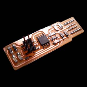
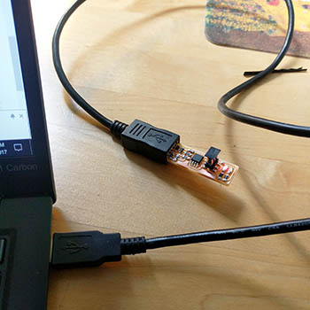
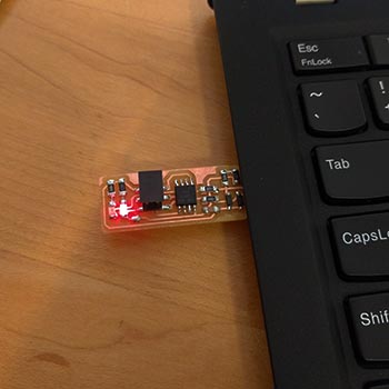
This week I've learned how to use the milling machine for fabricating a PCB (FR1: phenolic paper). During the electronics production training session led by Kreg Hanning, we used Roland Modela MDX40a Before moving into the fabrication process, as a group, we characterized the specifications of the PCB production process using the provided traces. Also, I did surface mount soldering (SMT) to build a FabTiny using a ATtiny45 chip and programmed it via USB connector.
Characterization of the PCB production
 |
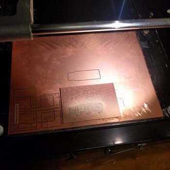
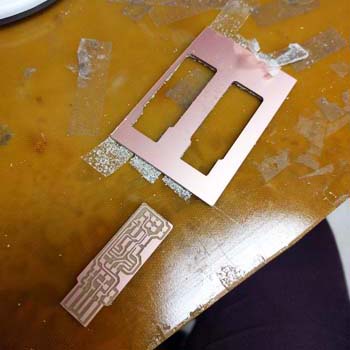
In order to specify the characteristics of the milling machine with the 1/64'' endmill, as a group, we fabricated the given traces and the result is shown on the top figure. The first three nodes from the left side of the traces were not well milled out. It turns out that the quality of the result is depending on the gap between the board and the tip of the endmill.
PCB Fabrication
 |
 |
 |
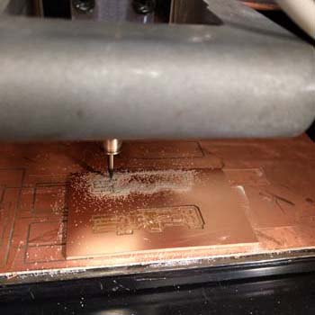
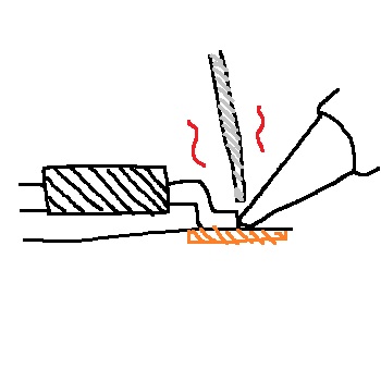
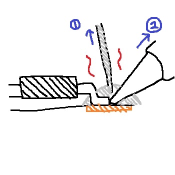
In order to hold the PCB on the milling machine workbed, I used a double-sided tape on the back side of the PCB and sticked it to the top of the sacrificial layer that clamped on the workbed. Using the mods, first I milled the traces of the circuit with 1/62'' and used 1/32'' for the ourline. Before starting the milling process, I had to make sure the workbed was cleand to prevent the misalignment. I adjusted the endmill height with set screws to make it slightly touch the surface of the PCB. When I tried first time to mill the traces, I found that the endmill was not touching the surface properly so had to stop it and adjusted the height and restarted it. In order to set the milling startpoint, I used mods to manipulate the origin of the workspace.
 |
 |
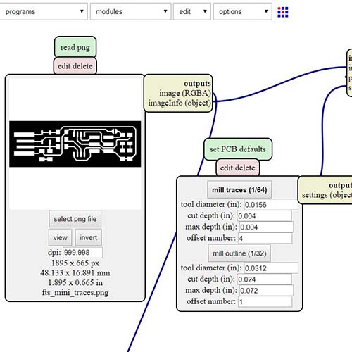
The mods setting for milling machine is shown in the top figures. It is important to know that the higher resolution (1000 dpi) of the trace PNG file make the better quality of the result.
 |
 |
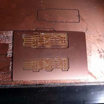
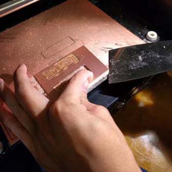
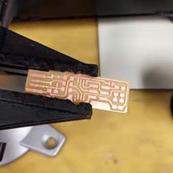
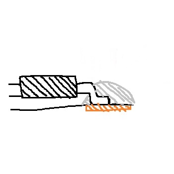
Once the milling of the outer trace is done, I took out the PCB board using a scraper and cleaned out the double-sided tape on the bottom surface of the board.
Cleaning
 |
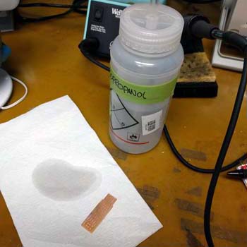 |
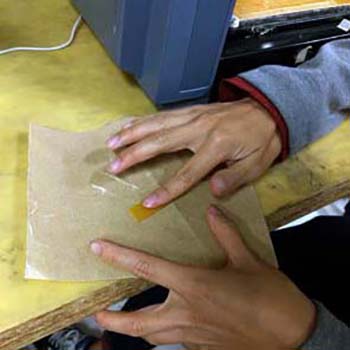
Since the copper surface of the board had some stains, I used a sandpaper (200 GRIT) to slightly glind out the copper surface and wiped out using isopropanol as Kreg recommended. Once it's done, the dust and residues from the copper trace were removed.
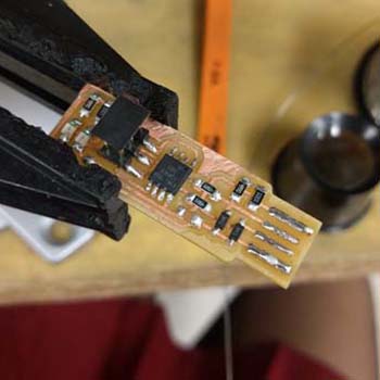
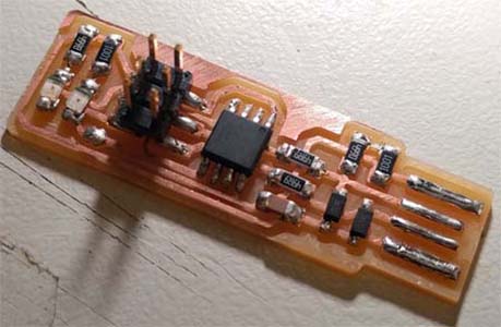
Assembly: Surface-Mount Soldering
 |
 |
 |
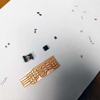
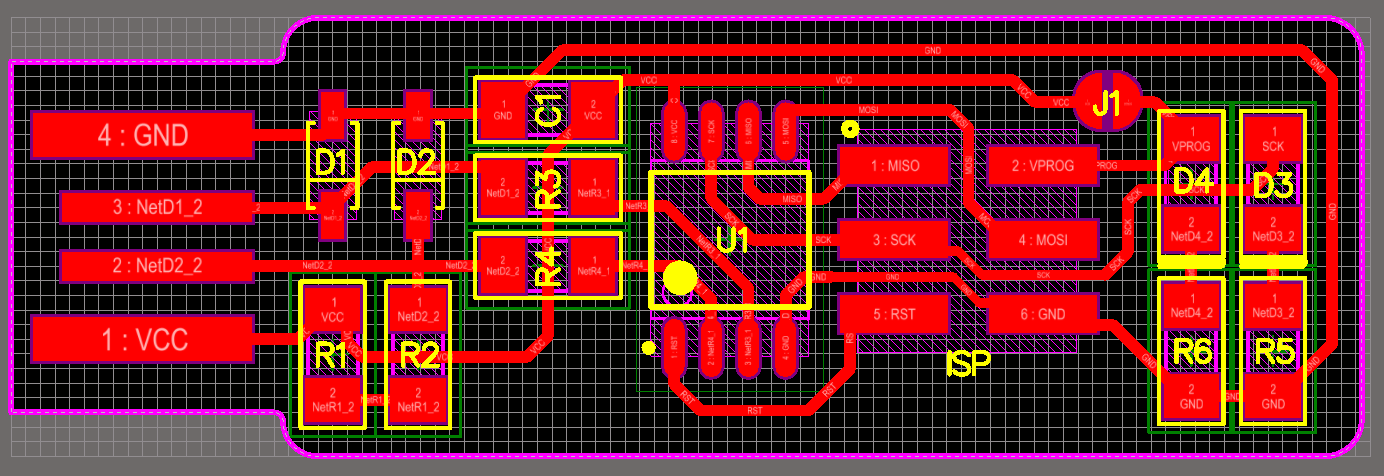
The design of this PCB board has no through hole and it consists of surface-mount soldering pads. The circuit designed by Brian requires the following components.
 |
 |
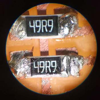 |
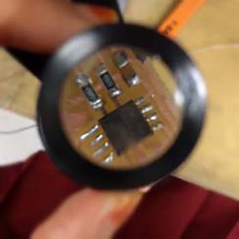
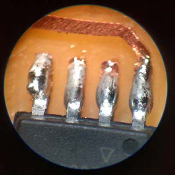
The soldering process took about an 1hr 30min for me. Sometimes the lead did not well stick onto the surface of the trace and just melted around the soldering iron tip. It was because the copper pad was not heated well enough to flow the melted lead. I had to place the soldering iron about 1 min to heat the component and the trace up. Before place the component on the board, I soldered the one of the pads and then placed the component on top of that. I used a twizzer to hold the component while heating up the soldered pad and the component leg. Once the soldered bulb was melted, the lead was solidified quickly so that hold the component.
 |
 |
 |
To solder the rest part of the component, I heated the component and the copper pad with the soldering iron (see the figures above) and placed the lead between the component and the soldering iron tip. Once the lead started to be melted and makes the small blub surrounding the component and the pad, I removed the lead first and the iron tip.
Dda-Da--!
 |
 |
Programming!
 |
 |