PCB Design
This week is all about going through the PCB design process from start to finish. We were given a picture of a circuit schematic and were asked to recreate the circuit, add some extra functionality, route it, mill it, solder it, program it, and test it.
The process of actually creating a circuit is almost completely foreign to me, which is massively embarrasing as a Course 6 at MIT (EECS). Granted, my focus is on computer science, but a complete lack of understanding of circuits is embarrasing.
To design circuits, it's a little more work than what I've previously done in classes like 6.004. In that class, there was a very nice browser environment called Jade that abstracted away the actual physical components and allowed you to add abstract electrical components like resistors, capacitors, and transistors to your circuit. However, when you actually want to be able to fabricate the circuit board once you're done designing it, there are some additional considerations you have to go through.
EAGLE
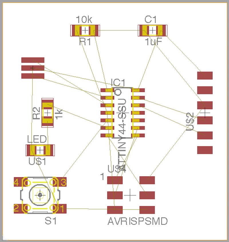
I did the circuit schematic and PCB layout design all in one program: EAGLE. While the program looked fairly intimidating, it wasn't actually terribly difficult to get a hang of. The flow of the PCB design went something like this:
- Start new schematic
- Add components you want to use to your environment
- Lay the schematic out and add electrical connections
- Import schematic into board layout mode
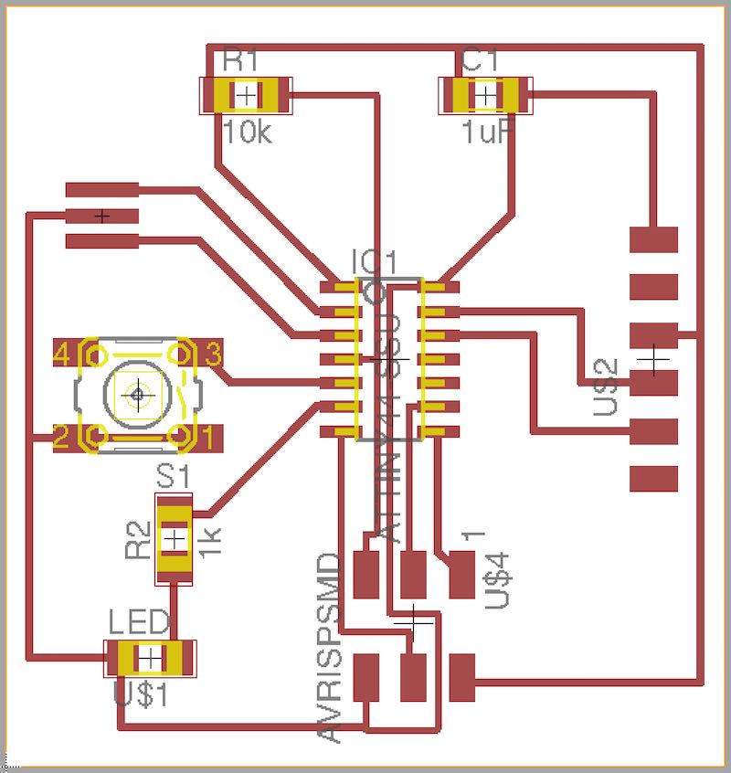
- Arrange components in the board layout
- Route the board
- Export Images import into Mods
Circuit Design
I followed this 3 part youtube tutorial series on EAGLE to get me started.
Some annoyances I ran into included:
-
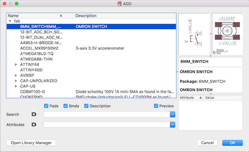
Finding the correct components for what I needed. There are massive part libraries that exist for suppliers like Adafruit and Sparkfun. Even though I was working within the "fab" component library, it was confusing to know which of the 3 resistors to use and how they all differed from one another. Additionally, the sames of some of the components seemed really foreign to me. While some like CAP and RES I understood meant capacitor and resistor, there were a lot of weird components like "CDBM1100-G" where I was just very confused. I'm sure I'll get used to this over time, though.
- Moving the components around. It is weirdly a massive pain in the ass to move multiple components around. After selecting all the components, you have to Opt-Right-Click and group move them, but if you don't click in the right place the selection will go away and you'll have to start over. I don't know why this has to be such a pain.
-
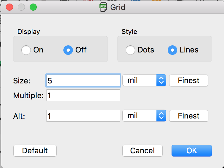
Grid granularity. So by default EAGLE has your board layout environment in mils (1/1000 of a inch ~ I didn't even know this was a thing). Similar to how "snapping" to gridlines, pixels, center, and edges works in adobe illustrator, EAGLE snaps to it's own grid. This grid, however, snaps only every 50 mils, which is a huge distance when you're trying to fit 3 tiny traces under an already small ATTiny44. I learned how to change this so it would only snap ever 5 mils, and when pressing the "control" key, I could move things every 1 mil.
- Trace width. It was hard to know what an appropriate trace width was. I started off using 16, but found that it was too tight to fit all the traces under the ATTiny. So I wanted to convert a trace to 12, but I couldn't find an easy way to select a whole trace path to change the width. So typically ripped up my route and rerouted with the smaller trace. There's also definitely circuit theory and physics I don't completely understand about how wide a trace should be for carrying certain amounts of current. But I generally tried to keep the widths as wide as possible to stay conservative.
-
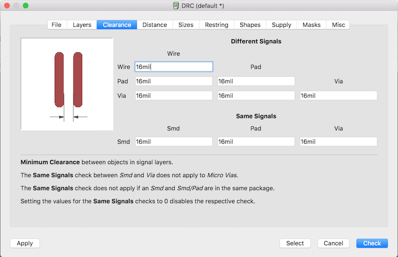
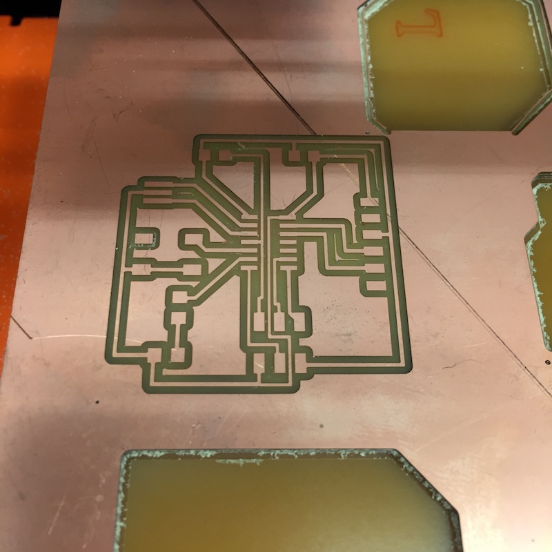
Clearance between traces. The problem is that in order to create the PCB, you have to mill around the traces on your board layout. This means the tool you use (1/64" endmill) has to fit between the traces. At first I was just eyeballing the traces to keep them somewhat separated. I'd export the image into Mods and after calculating the tool path, I'd see that there were multiple traces too close together. Then I figured out what DRC was. This panel, among other things, allows you to set the minimum distance (clearance) you need between traces, pads, vias, etc. A 1/64" endmill has a diameter of 15.625 mils, so I put the clearance at 16 mil. While this mostly works, the corners of traces sometimes add weird bulges that cause Mods to believe they're connected. So start with this and make any adjustments necessary. Again, always check the calculated toolpaths in Mods before milling.
-
Autotrace vs manual trace. There is an option to auto-route your traces given the component placement on the board. EAGLE will use some clever algorithm to figure this out. But generally it ends up not being exactly what you wanted, and ripping up traces they made is a large pain. So in general I stuck to manually routing, and I find it comes out just fine and is a good mental challenge to figure out how everything has to be layed out.


Making the Board:
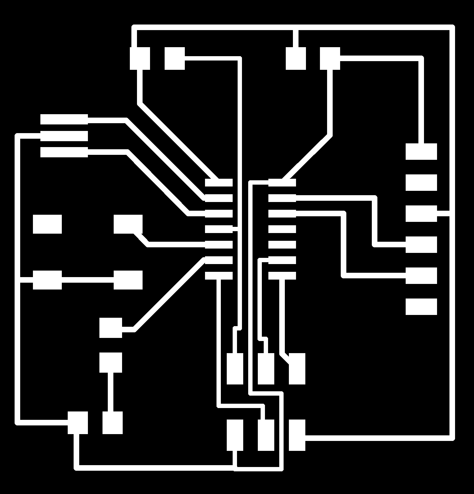
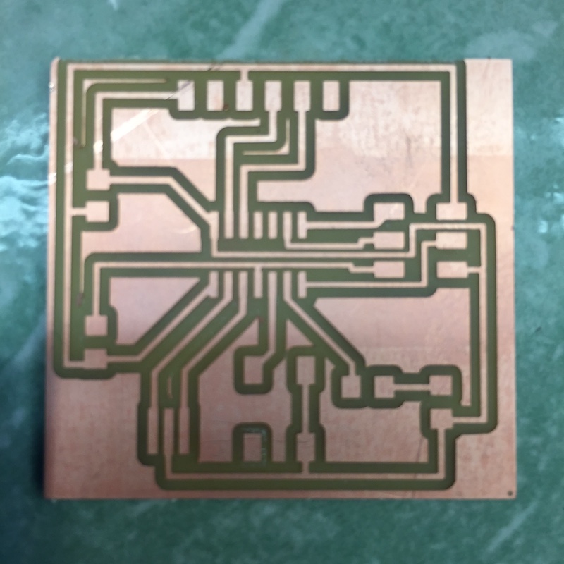
When your board is all layed out how you want it to be, it's time to actually mill it out. To do this using the Mods software I've been referring to, you need to create a high-resolution image out of the board traces and outline. To do this, you can toggle on different layers in layers settings, and just choose to show the top layer. From here, you can File, Export --> Image. I make mine 500 DPI, Monochrome, with the Full Area. This basically exports your whole board to an image. Choosing "window" area would export whatever is inside your EAGLE workspace window (whether that's more than or less than the whole board). I don't reccomend using that. You get a picture like this:
To export the outline of the board, choose to only show the dimension layer. To invert the colors of the board layout, go to Options --> User Interface. There you can choose to have a white background so your outline is black (when exporting in monochrome).

One problem I had with exporting the outline of the board was with the thickness of the outline. Sometimes Mods wouldn't pick up the outline if it was only 1px thick, so the outline really needs to be thicker than that. So I tried opening the outline export in Photoshop to add a little thickness to the line.
What I got scared about was adding thickness inside the image would possiblly mean the mill might mill over traces close to the edge. So instead I made my image an extra 40 px wider and taller (out of a couple thousand pixel image), and made the outer 20px black.

The issue with doing this was when milling my board, I realized my outlines image was bigger than my traces image, so the origins would be slightly off. I was already done with the trace milling, so I tried to compensate slightly by changing the X-Y origin of the mill to be slightly down and to the left to account for the extra 20px offset. While this wasn't ideal (and you'll see how close the cutout was to my traces below), it ended up working out. Moving forward though, I definitely need to find new technique for exporting good outlines.
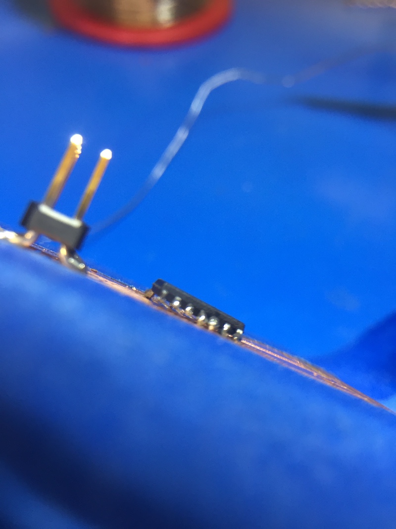
The home stretch is soldering the board. While I got some practice doing this during the Electronics Production week, I still had a lot of trouble doing this for this board.
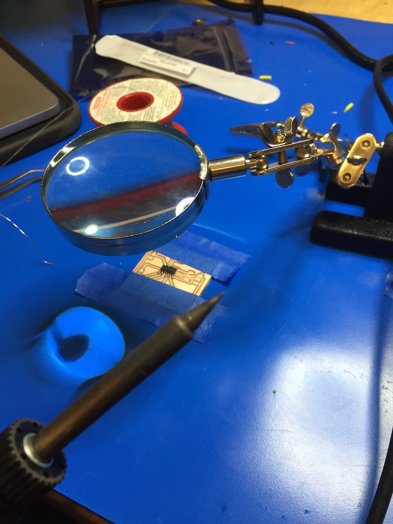
One problem I had was after soldering the ATTiny44, I turned the board to the side and realized it was kind of coming off the copper. This must have been a result of not pinning the board down properly for the first connection. If the first one is screwed up, the rest of them are going to be screwed up too. So while I had to desolder the whole thing, I'd reccomend just checking that your component is laying flush on the board after making the first connection.
To stay organized, I like keeping my components together, stuck on a piece of tape in a known order so I can work in the soldering lab instead of constantly going back and forth to the inventory room to get all the components I used.
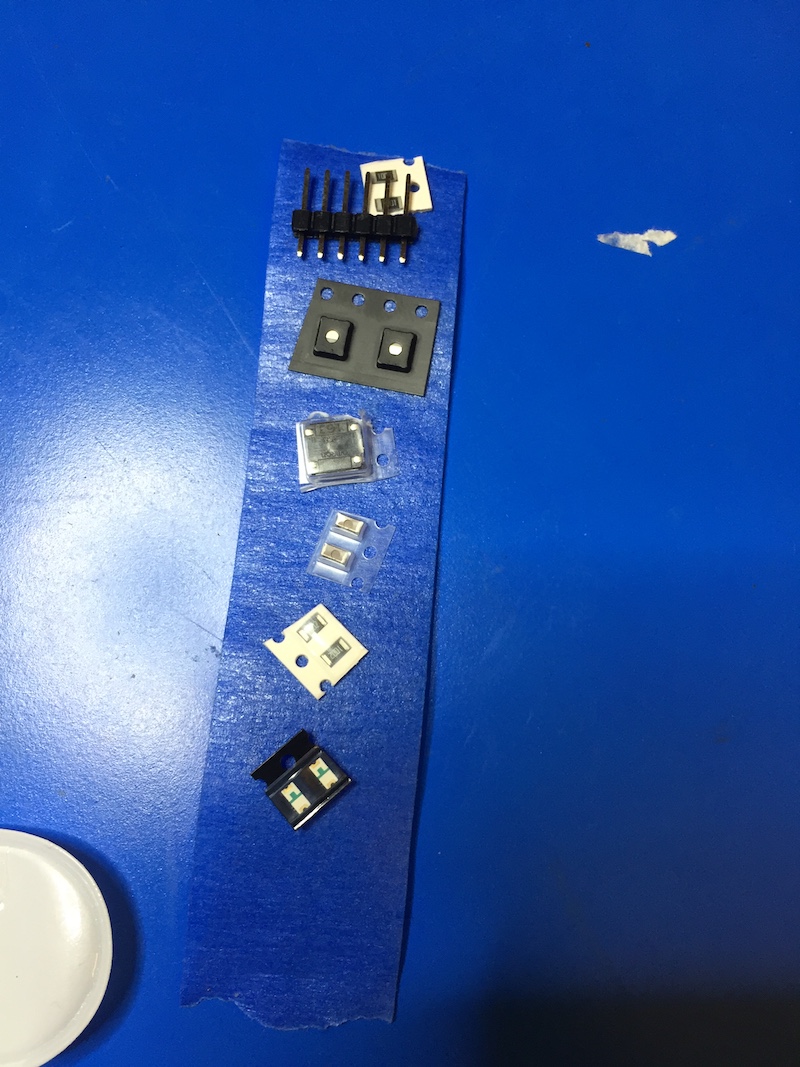
One last problem I had was making sure I knew which way the button (switch) was supposed to go on. The button looks
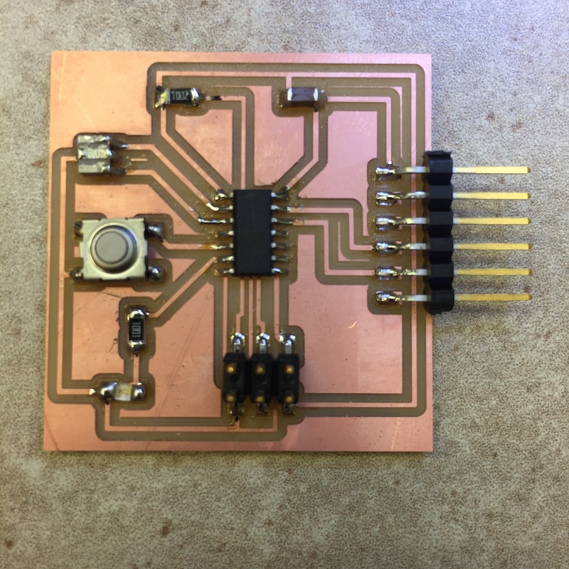
Finally, the board turned out like this:
Testing the Board:
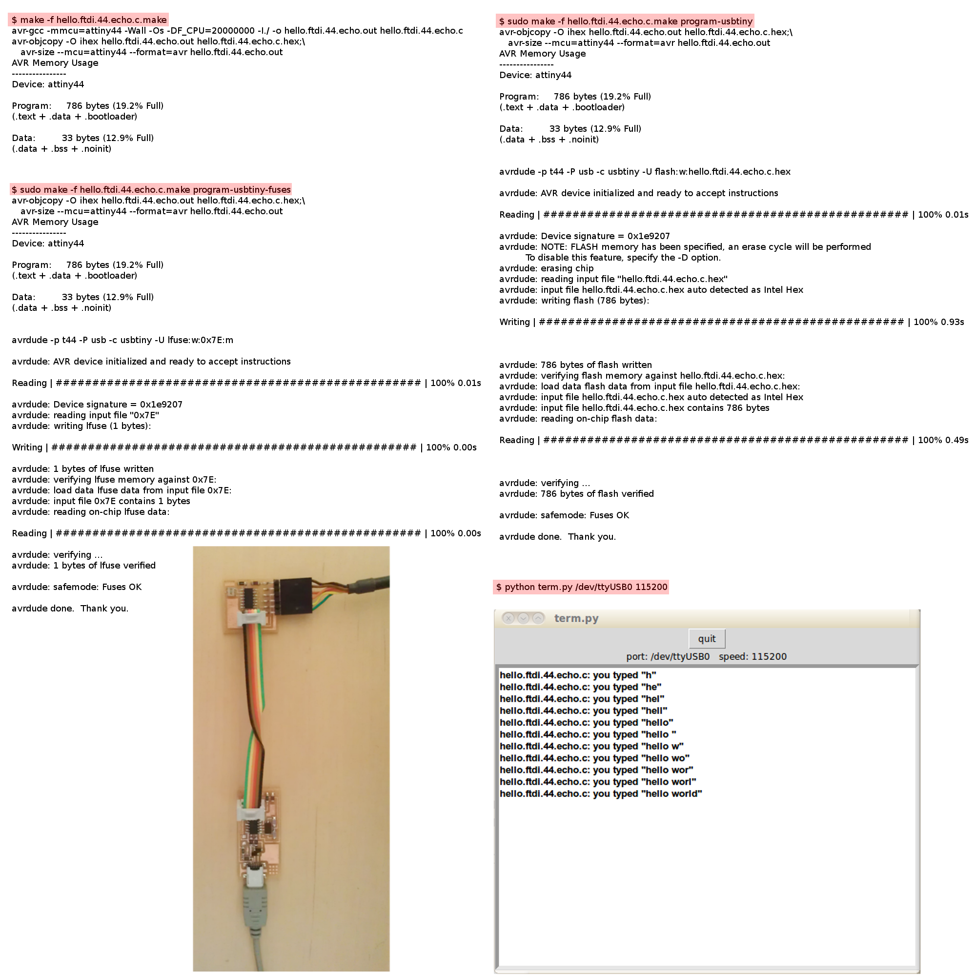
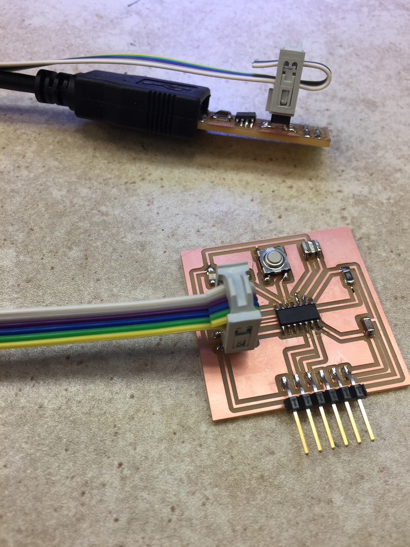
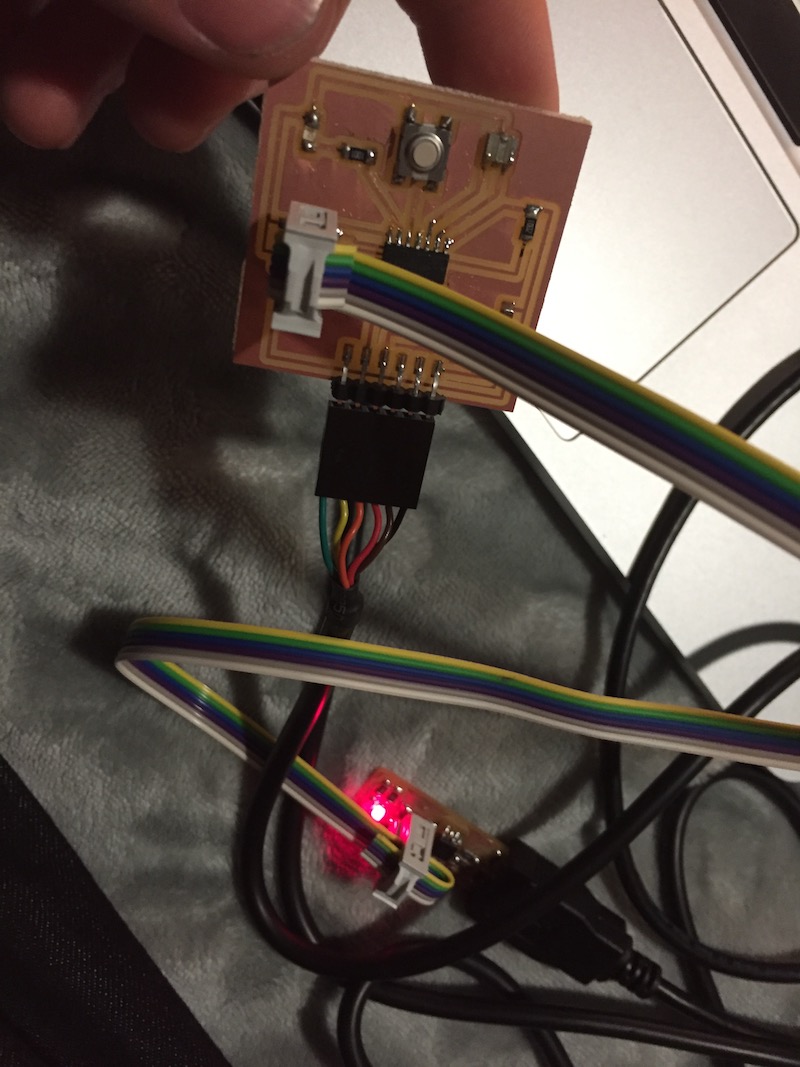
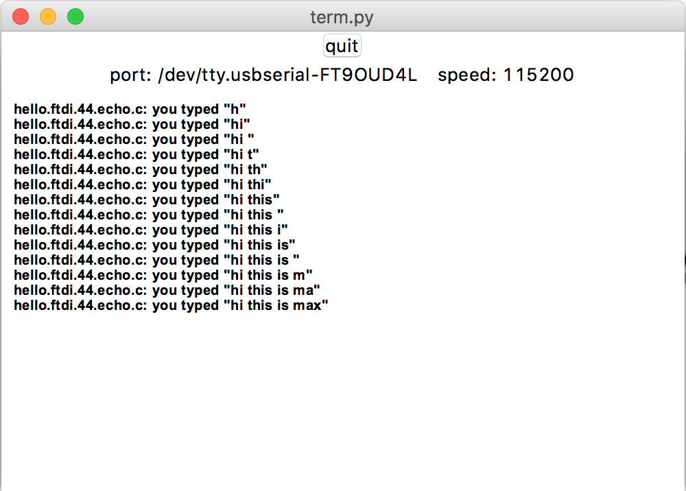
The last part was to try and program the board. I wasn't really sure how to go about doing this, but I combined the process I did to program the FabTinyISP (in terms of using CrossPack) and this photo of programming Neil's echo Hello World board to compile Neil's hello.ftdi.44.echo.c file and load it onto my board. Suprisingly, it worked!!
Terminology
Schematic, Board Layout, Net, Trace, Trace Width, Board Layers, Grid, Clearance, DRC, ERC, mil vs mm, autotrace, makefile
Technologies Used
EAGLE, Roland Mill, TinyFabISP, C
Resources Used