Assignment: Redraw the echo hello-world board, add a button and LED, make it, and test it.
Design
This week we take a step up from just milling and stuffing an existing PCB design to designing our own PCB. Well, design in this case is pretty straightforward, just having to add a few components.
I started with the example board layout, which shows the starting components and one layout of wiring them together. I used Eagle for this assignment, since we got a nice walkthrough in session, and it runs for free on Linux. (I got it up and running in my Chromebook really easily!) I imported the FAB parts library. I’m really glad that we have this compact inventory, because otherwise I would have no idea what to make of the intimidatingly large assortment of components out there. I added all the components to my schematic, but the clock ended up being tricky because it was categorized as “resonator.” I wired up the parts directly. On this first go, I actually drew in all the wires with the net tool because I wanted to make sure I understood how it all fit together. But I can definitely see how horrifyingly messy this would get with scale and why the naming and labeling to connect wires would end up being really useful.
One of the initially most frustrating things about Eagle was moving parts. I could move around my little parts like LEDs and capacitors, but I frustratingly couldn’t get the larger parts to move – in either the schematic and the board. I’d right click and wouldn’t get a pop-up menu, or I’d try to drag them while in the “move” tool. It turns out that in Eagle, every part has a little + in the center, and you can only really interact with it (right clicking and dragging/moving) on this little plus sign. Things got much easier once the TAs helped me figure this out.
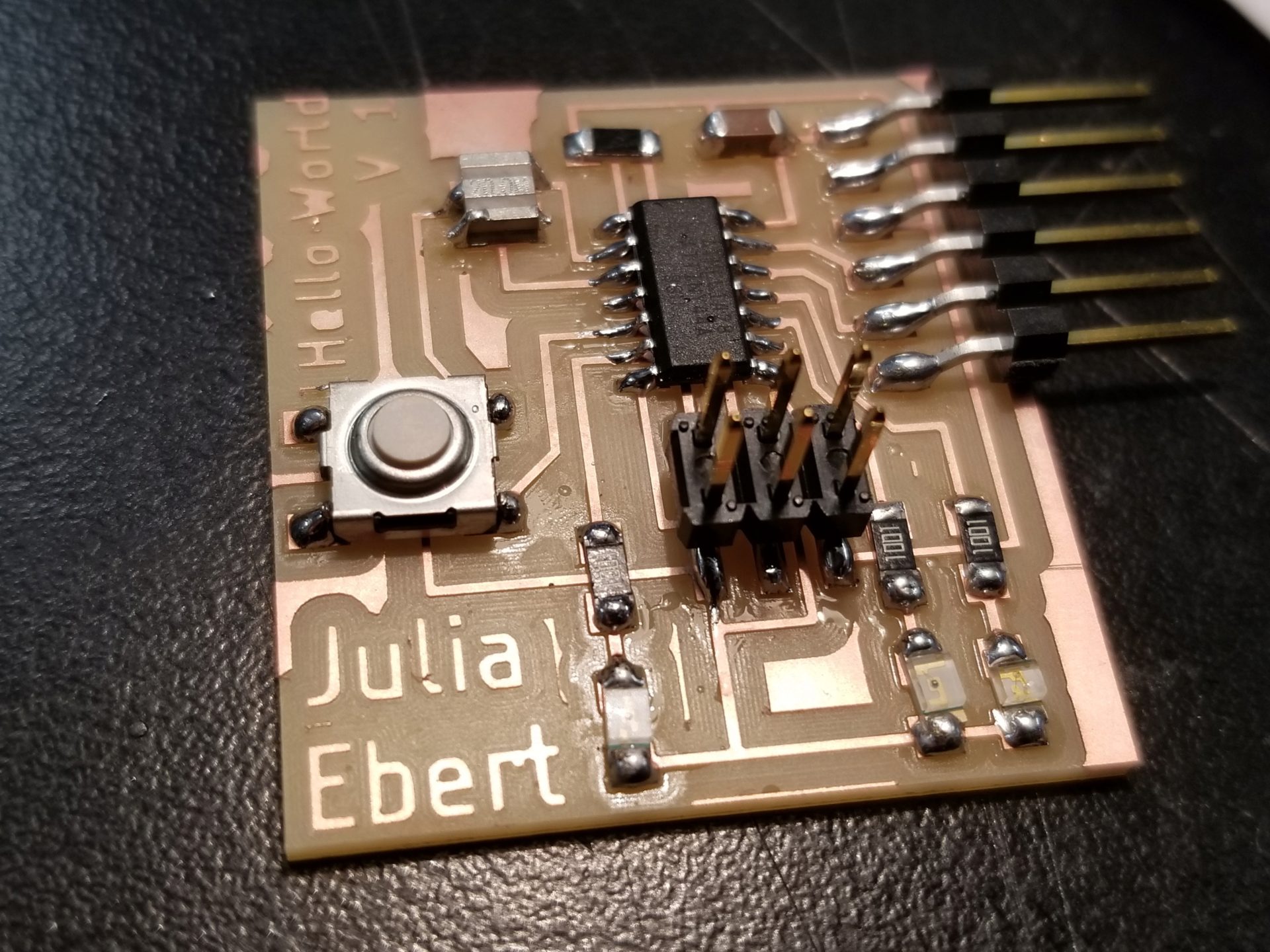
In addition to my mandatory button, I added 3 LEDs to my design, each connected to a 1 kΩ current-limiting resistor. I could have used the RGB LED in the FAB library, but that’s not nearly as much fun as getting to solder on more tiny LEDs for practice. Plus, this way I don’t have to decide yet what colors I want to use and I get to use up all the spare pins on my ATtiny 44.
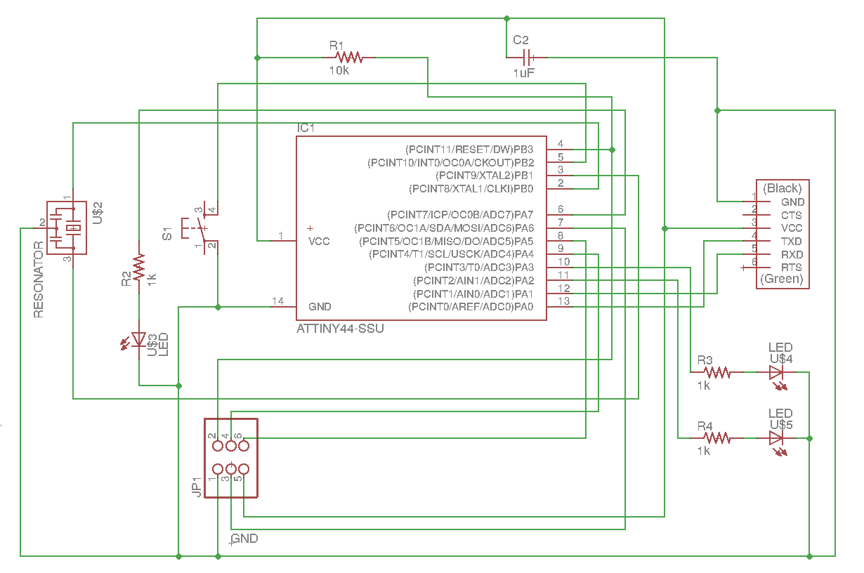
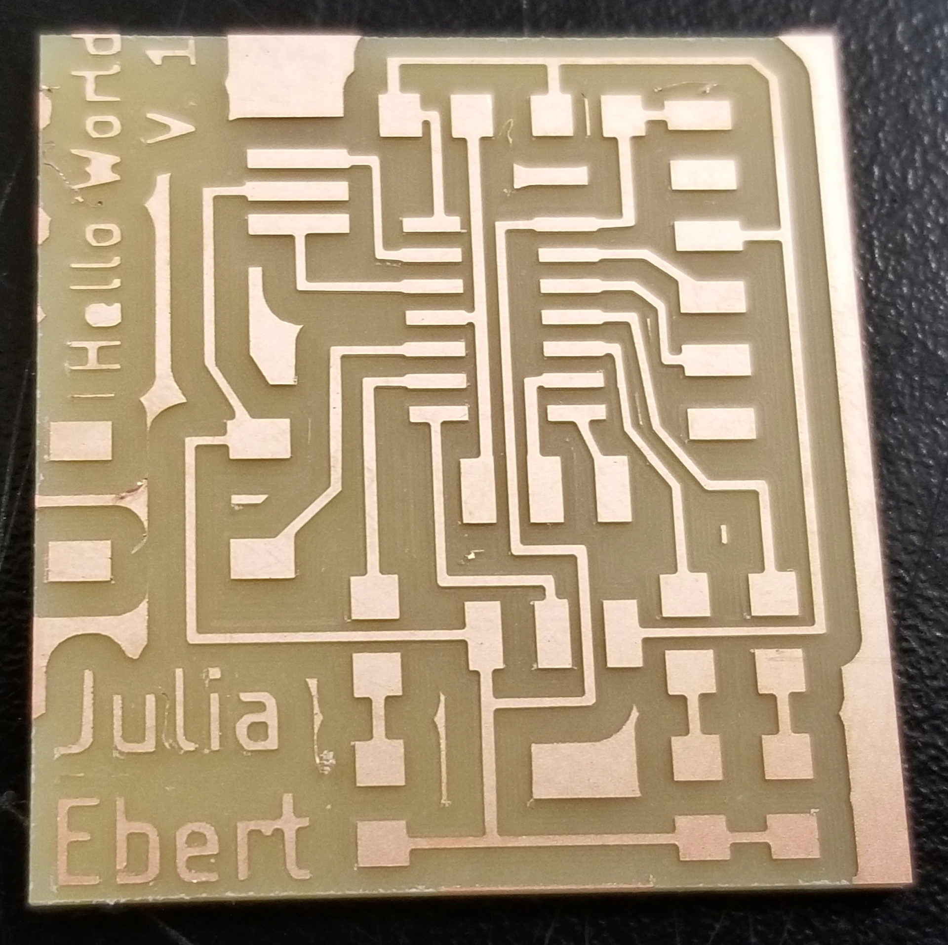
After finishing up my schematic, I moved on to laying out the board. I mostly stuck following the example board when it came to route traces, since I don’t have a good intuition yet for how to lay things out. Initially my LEDs were all over the place, but I figured out a way to nicely line them all up along the bottom. I wasn’t certain what thickness to use for the traces, but based on the characterization part from Week 3, I decided to start with a thickness of 0.012 inches. I did make the mistake of not setting the trace thickness before starting to draw them all in. Luckily, I could change them after. From the toolbar, I selected Change (the wrench) > width, and selected 0.012. (Frustratingly, there are no units listed.) I could then click on all the traces I wanted to change, and any I added after that would use this new width. In adding the LEDs, though, I ended up placing some traces that look pretty janky.
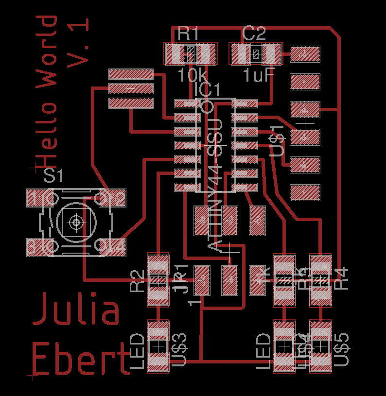
While adding the traces, I primarily used a grid size of 0.005”, which allowed me enough fine-grained control but let me still draw nice vertical and horizontal lines. However, I did intermittently switch the grid size to 0.01625” (1/64”) and turn grid display on so I could check that I’d left enough space between traces for the endmill size. Toward the end, though, I figured out a cleaner approach: set the grid size to 0.00390625” (1/64/4”), then set the multiple to 4 and turn on display. This way I could keep checking the spacing but snap to a grid 4x smaller than the endmill, which gives a lot more flexibility.
I also added some text to the layout, just to try it out. Adding “Hello World V. 1” might actually be useful, in case I have to redo the board and don’t want to get them mixed up. But adding my name? That’s pretty much just narcissism. I’m not totally sure how well these will cut out, since the spacing between letter parts looks pretty tight. Hopefully it will at least be intelligible.
I also needed to create an outline of the board. I used the rectangle tool and drew an outline in the “Dimension” layer.
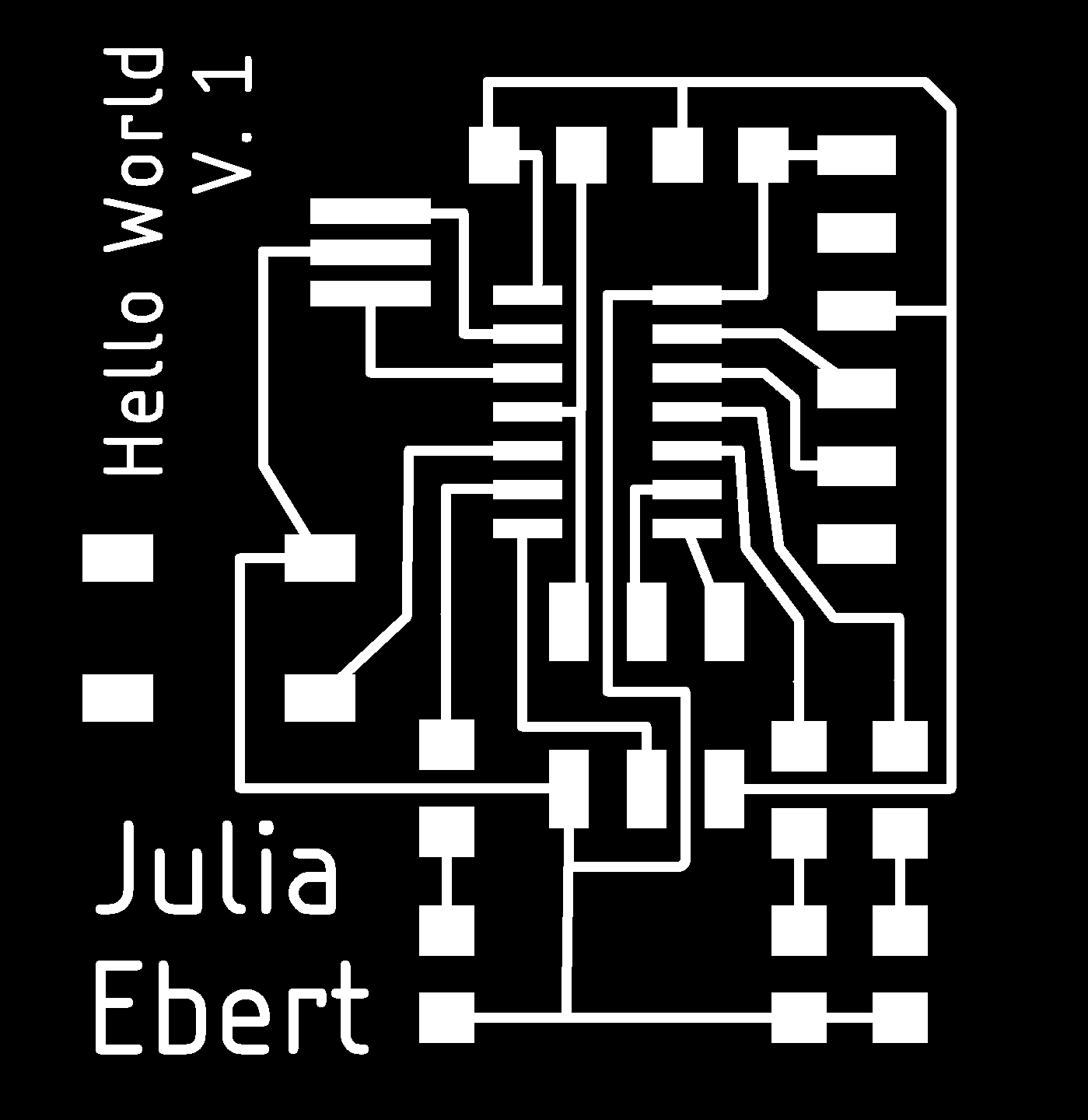
Finally, I had to turn it into PNGs for the mill. I turned off all layers but “Top” (for the traces), then went to File > Export > Image. I checked the monochrome box, set the resolution to 1000 dpi, and saved. For the outline, I turned on only the “Dimension” layer and exported it in the same way to another image file. At this point, I should theoretically be all set to mill the board.

Production
I milled my board using the same process and mill as in electronics production week. After getting Rob’s help to fix a mysterious issue where Mods wouldn’t connect to the mill, everything went flawlessly. I used more double sided tape than last time to keep things flat. I also set the depth for cutting the outline to 1.7 mm to help save the sacrificial layer.
Before actually milling, I double checked the preview of the endmill path. To my relief, I had left plenty of space between the traces. As expected, the small lettering of “Hello World” didn’t get fully cut out, but that’s fine – at least my name looks nice. My trace thickness also seemed good – not too thin to delaminate, but not so thick that I couldn’t route things well.
Soldering the board also went quicker than electronics production week, as I’m getting the hang of it. I’m pretty sure I didn’t solder the microcontroller on backwards this time, for example (though it was hard to tell which was the correct orientation). The resonator/clock was also kind of weird to attach, since the pads go primarily under the component.
Programming and Testing
The class website was really unclear on how to actually program and communicate with the board, but with the help of Rob and our TA Brian Plancher, we finally figured out all of the pieces. I thought I’d share it here so others wouldn’t have to go through that confusion. These directions are based on using a Linux machine with all the necessary software installed that’s described last week. I used the Chromebox running Gallium in the Harvard SC102 shop (next to the Formlabs printer).
Connections
- Connect your programmer (from last week) to the computer by USB.
- Connect your Hello World board to an FTDI cable, plug the FTDI cable into USB on the computer. (The board is powered through the FTDI header, so you need to do this to program it, even though you’re not talking to the board by FTDI yet.) Before you plug your board into the FTDI cable: check the orientation of the FTDI pins. Pins 1 and 3 are VCC and GND, so you can use a voltmeter (multi-meter) to check that you see 5 V between these pins. (Your FTDI cable needs to be connected to USB power, and you have to plug in some header pins into the FTDI end to touch to the multi-meter.)
- Connect the Hello World board to your programmer with the 6-pin header cable. (Make sure you’re matching pins - e.g., ground connected to ground.) The red LED on your programmer should light up.
Programming your Hello World board
You’ll need to download the C program and the Makefile to program your board. You can look at the makefile to see the different command options it can run.
- Open a terminal and navigate to the directory where you downloaded the program files. (Use the
cdcommand in Mac/Linux.) - Check that your programmer and Hello World board are connected and detected with
lsusb. The programmer should show up as something likeMultiple Vendors USBTinyand the FTDI cable asFuture Technology Devices International .... - Compile the program:
make -f hello.ftdi.44.echo.c.make.-ftellsmakewhich file to use as the makefile. This will create a.hexfile that can be sent to your board. - Send the file to your Hello World board:
make -f hello.ftdi.44.echo.c.make program-usbtiny - Set the clock on your Hello World board:
make -f hello.ftdi.44.echo.c.make program-usbtiny-fuses
At this point, your board should be fully programmed, so go ahead and disconnect the programmer from your board and from the computer.
Communicating with your Hello World board
- Download the Python terminal for communicating with your board through the FTDI header.
- Check what port your Hello World board is connected to. Look at the output of
ls /dev. This shows the devices connected to your computer. There should be one listed as something likettyUSB0(or some other number at the end). That’s your board. - From the directory where you downloaded the terminal, run
sudo python term.py /dev/ttyUSB0 115200(or wherever you determined your board is connected). The115200is the baudrate of the device, which was set with theprogram-usbtiny-fusescommand we ran earlier. - A terminal window should pop up. Type a single character, and you should see a response from your board like this:
you typed "a". If you want to reset the list of characters, unplug your board from the FTDI header. (If you unplug the cable from the computer, the/dev/ttyUSB*location might change.)
Troubleshooting
There are a lot of places that this can fail along the way. If it does, here are some things (a non-comprehensive list) to check:
- Verify that your devices are connected/detected by the computer with
lsusb. - Check that you have the right permissions to run what you’re trying to run. (For example, don’t forget to run the serial terminal as root with
sudo.) - Use a voltmeter to check that you’re getting power where it needs to go on your board.
- Use the “beep test” on the multi-meter to check that things that should be connected are, and that you haven’t accidentally created any shorts. (Check your soldering if either of these occurs.)