Computer-Controlled Cutting
week 2 (09/19 - 09/26)
{machine: Speedy 100 Flex Laser Cutter}
C. Microfluidic Chip Fabrication
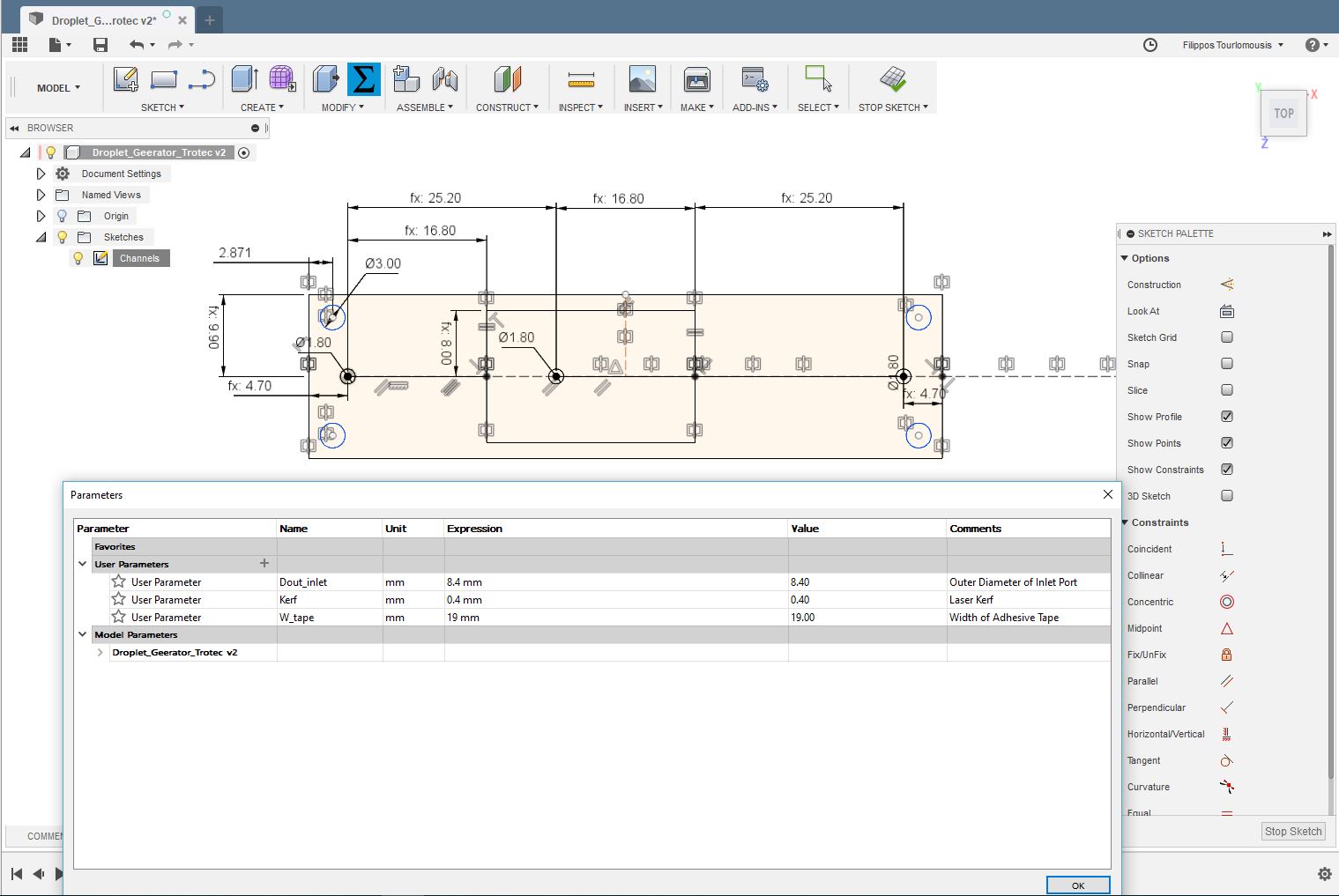
i. Parametric Design Workflow in Fusion
ii. Corel Draw Design Workflow
i. Study 1: Power with Focusing
ii. Study 2: Power with De-focusing
Laser Machining: Rapid Prototyping of Droplet Microfluidic PMMA Devices
Summary
This week's topic is Laser Machining. The assignment is to design and fabricate a snap-fit construction kit made from card board. I slightly deviated and decided to work with PMMA or in other words acrylic. Specifically, I wanted to come-up with a workflow for rapidly fabricating multi-layer microfluidic devices (MFDs). We have been awarded a NIST grant and time is running out for the first phase after which we have to build and demonstrate machines for high throughput materials synthesis and measurements. The goal is to make these technologies accessible to the masses through the global network of fab labs. So, this is a great opportunity to dig a little deeper into laser machining and push the fabrication limits of a readily available laser cutter. My design is a simple two layer droplet MFD with the lower layer containing fluidic channels, inlet, outlet and alignment holes. The upper layer contains only alignment holes for guiding the bonding of the two layers and closing the device in a leak-free manner. Specifically, the bonding of the two layers is challenging due to the nature of the material and the ablation process. To achieve leak-free bonding I tried to bond the two layers using a solvent-activated double adhesive tape. I run several parametric and characterization studies to understand the process resolution with respect to depth, width and profile of the engraved channels. The results were very promising! Below you can see images of the individual layers and the final assembled device. While the device allowed efficient fluid transport (see image below), I have to do more work to finalize the assembly-bonding workflow. Scroll down to read details about the workflow and challenges and how I plan to overcome them. I will continue working on perfecting the chip fabrication workflow throughout the course! Stay tuned!
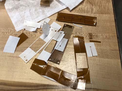
Layers
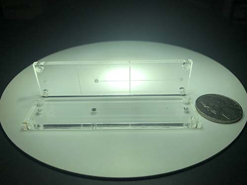
Assembled Multilayer Device
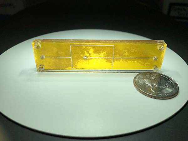
Assembled Multilayer Device perfused with Water + Blue Food Coloring

Intro - Motivation
The capital requirements to prototype a conventional photolithography-based microfluidic device are high. Photolithography requires an extremely clean environment and a UV exposure system suitable for contact lithography. The photoresists and solvents are also a significant expense. After replication molding of a lithographic master into PDMS, the device is activated with an oxygen plasma cleaner, another high-cost device. With the appropriate equipment, lithography and PDMS can achieve resolution down to ~1 μm for between three and forty times higher capital cost than the procedure described here. We are presenting a low-cost method to build microfluidic chips with resolution on the order of ~100 μm. Several low-cost approaches have been demonstrated to fabricate devices for droplet microfluidics. These include paperfludic approaches, thermoplastic fabrication, optical adhesive bonding, glass etching and 3D printing.
Our method uses PMMA which has advantages over PDMS for generating and maintaining droplets. PDMS is an elastomer widely used in droplet microfluidics. However, its surface properties are variable and change in contact with different organic solvents. Furthermore, PDMS is permeable to water28. PDMS can also absorb hydrophobic small molecules. Many experiments require time-consuming, expensive surface treatment. For the laser machining assignment I chose to work with acrylic as a material instead of cardboard. Specifically, PMMA is a thermoplastic material with excellent transparency, biocompatibility, non-porosity, durability and low-cost availability. PMMA has attracted the attention of the microfluidic community. However fabrication in PMMA is not as easy as PDMS. It is not elastomeric and not easy to cast. It can be cut with a CO2 laser35, and several bonding methods have been reported, i.e., adhesive bonding36, solvent bonding37, and thermal bonding. However, adhesives and solvents can occlude the channels and introduce additional (potentially unwanted) materials to the device. High-pressure thermal bonding requires an expensive heated press (e.g., a Carver press costs more than $9,000).
Microfluidic Chip Fabrication
A 1 mm thin cover layer (Extruded XS Acrylic, Aliexpress) and a 2 mm thick channel layer (Plexiglas®, Tri-State hardware) were etched and cut to form microfluidic chips. Supplementary Fig. SI1 shows the assembly for bonding the microfluidic chip components. LaserDRW software was used to create the designs for all chips. A K40 type laser cutter with a 40-watt CO2 laser tube was used to cut the designs into the acrylic. Model F-LM1390, by FLM, China was used for this study; comparable K40 cutters are available from various Chinese manufacturers sold on Amazon and eBay. These laser engraver/cutter devices should be treated with extreme care. Laser safety precautions must be followed including laser safety goggles and good ventilation. The device should be regarded as a laboratory or research grade laser, not a consumer device. In the design, access holes were cut first; the deepest channels were then etched to a depth of 600 μm, and shallow channels were etched last by increasing the laser head translation rate. After the channels were etched, the chip was cut free from the bulk material. The acrylic plugs left in the access holes were punched out with a blunt syringe needle. All features were cut into the thicker 2 mm acrylic (unless otherwise specified). The 1 mm thick acrylic was then placed over the top to seal the channels. Paper spacer was placed around the perimeter of the press to aid in uniform pressure distribution on the chips placed at the center of a heated platform. A spacer of 32 sheets of paper with an uncompressed thickness of 3 mm was used. The whole assembly was then placed in a heated press (Promo Heat, Tamarac, FL, Model HP230B) at 145 °C for 10 minutes under ~60 N of force from the mass of the press plus the applied force on the handle (measured with Vernier force probe). For a schematic and image of the press and assembly, see Supplemental Information Fig. SI1.
The Laser Cutting Machine: Trotec_Speedy_100_Flex_Laser_Cutter
Parametric Design Workflow in Fusion
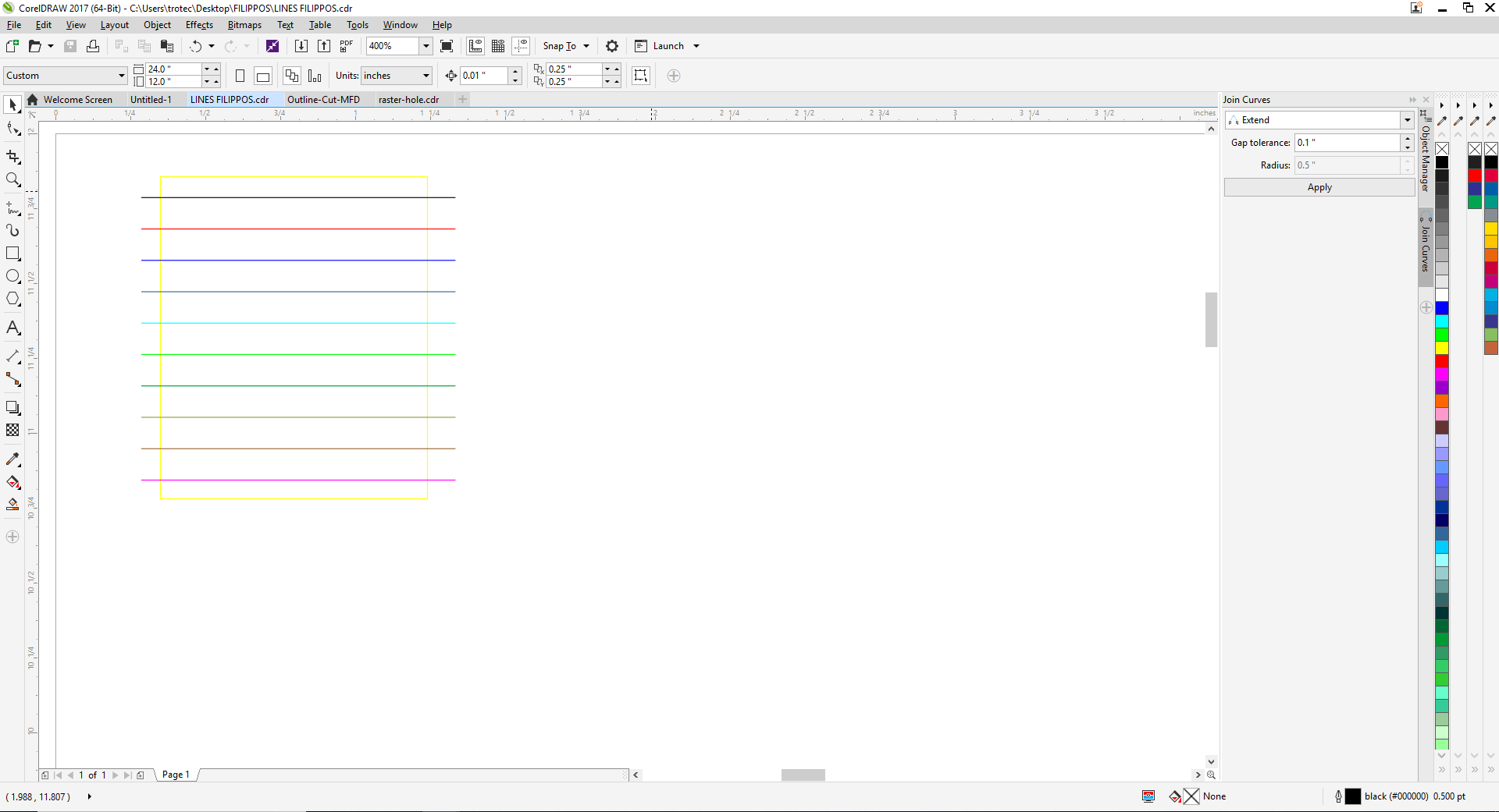
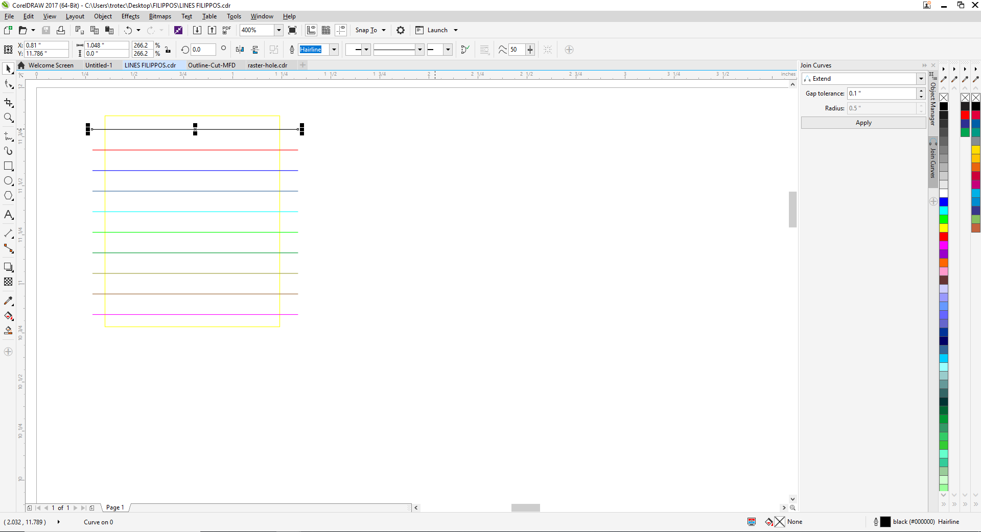
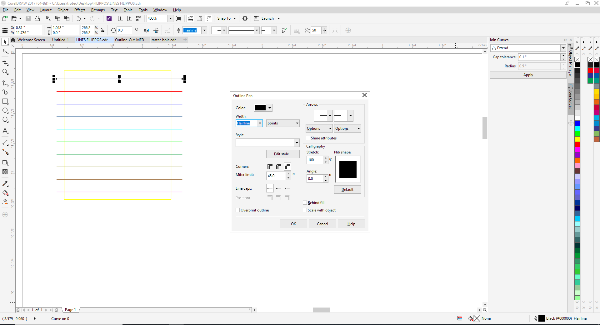
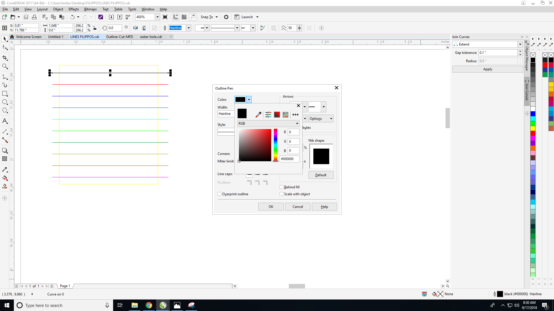
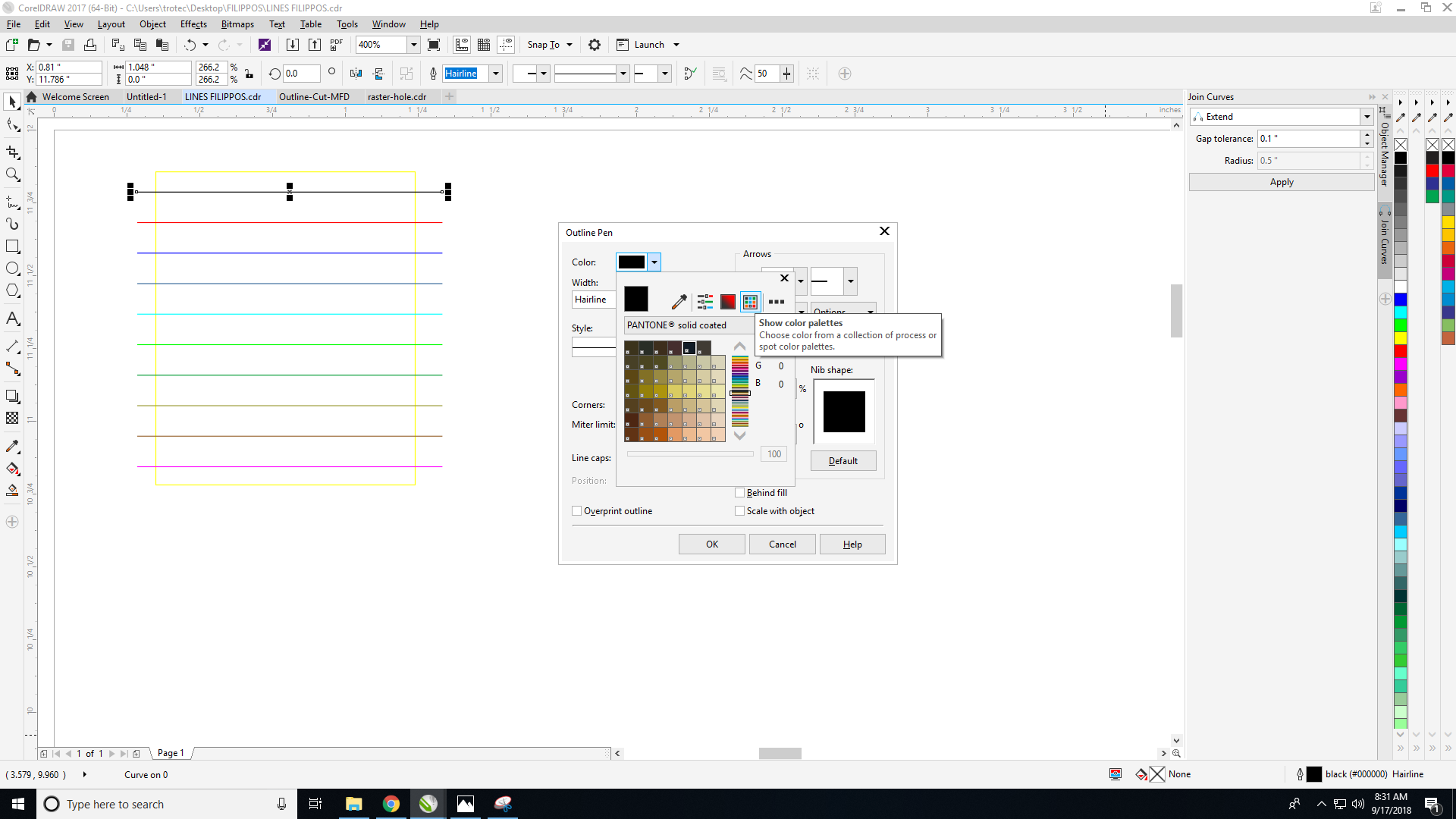
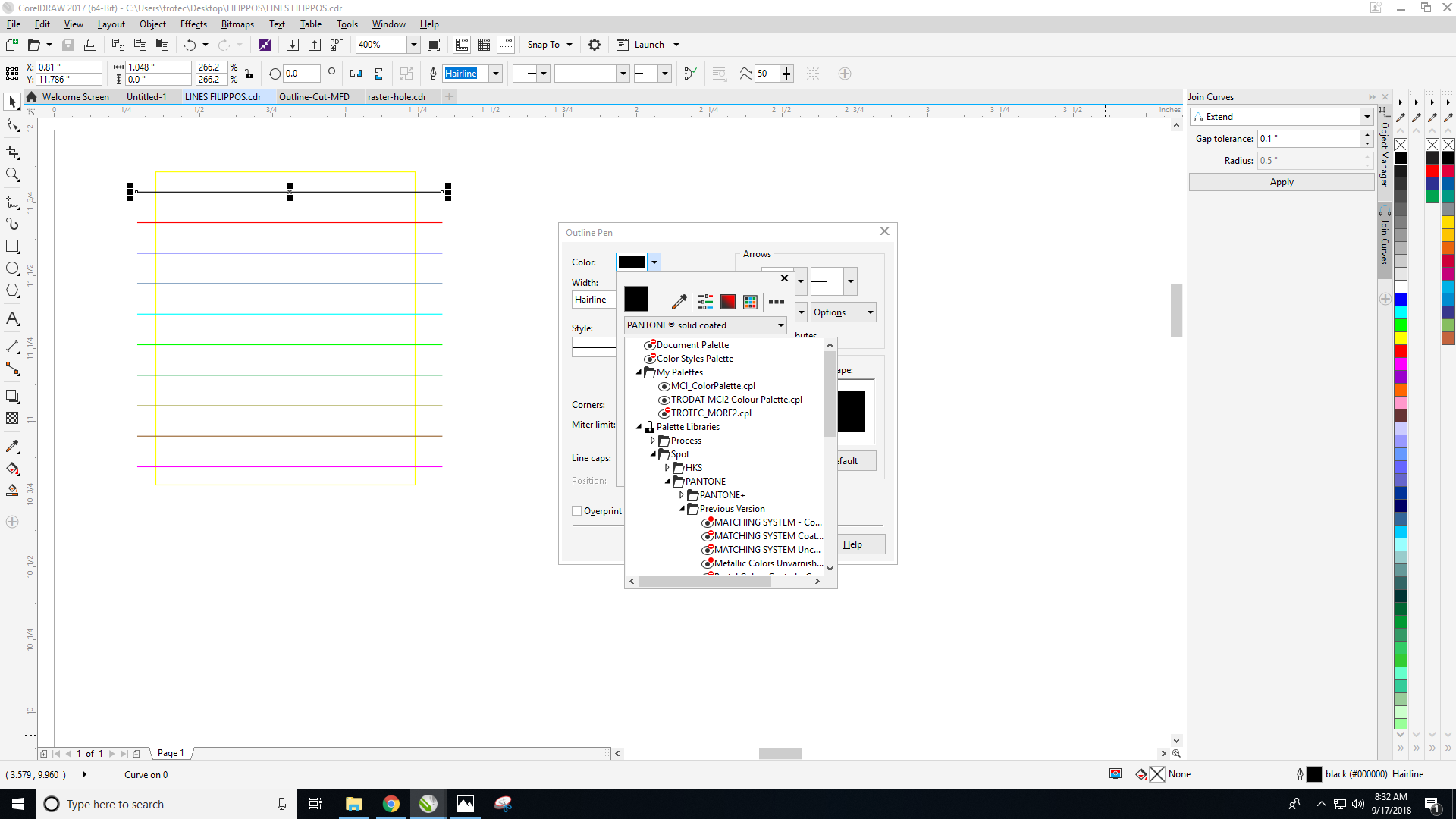
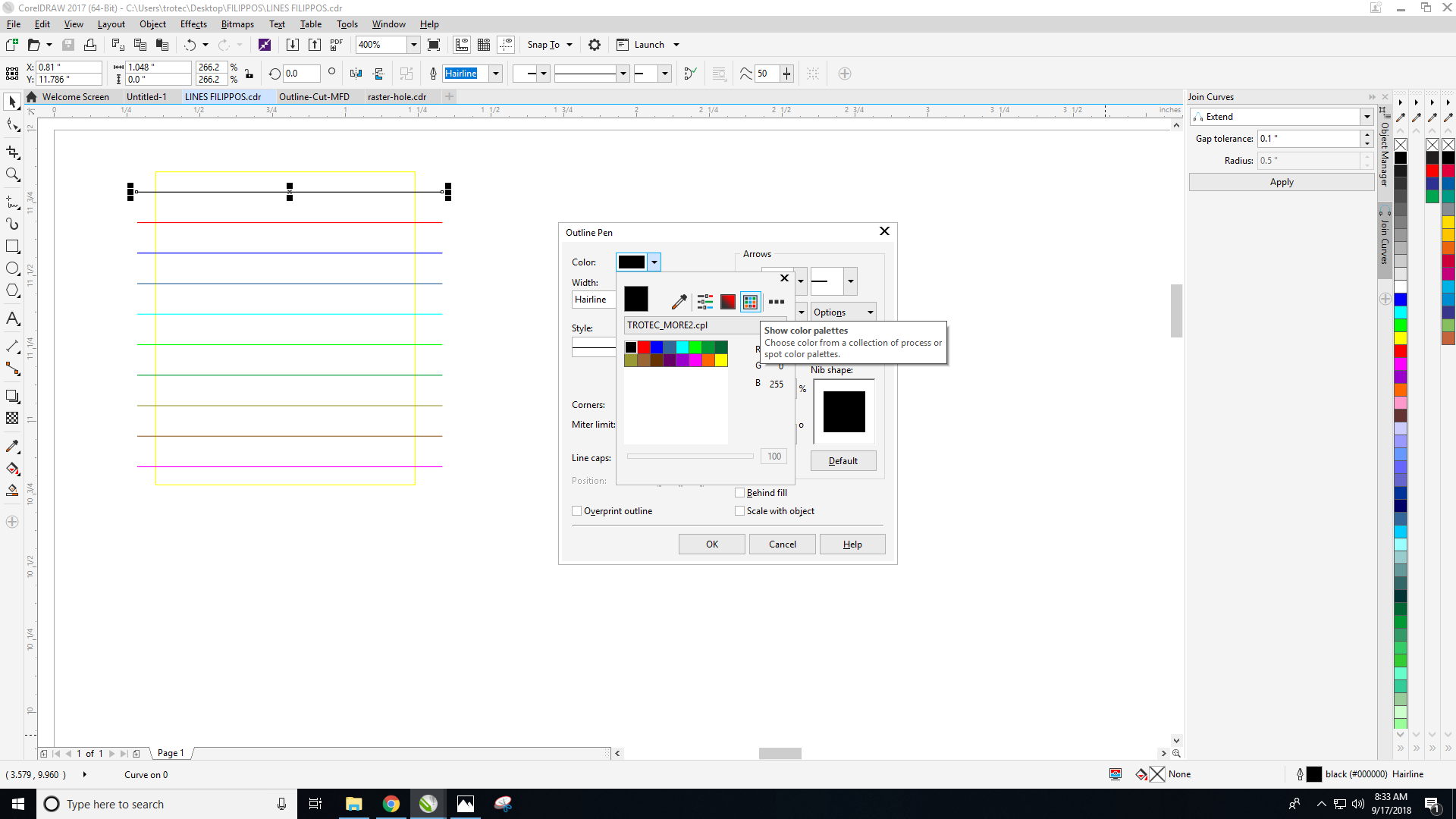
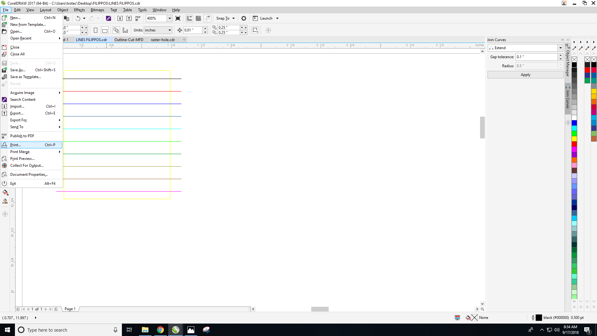
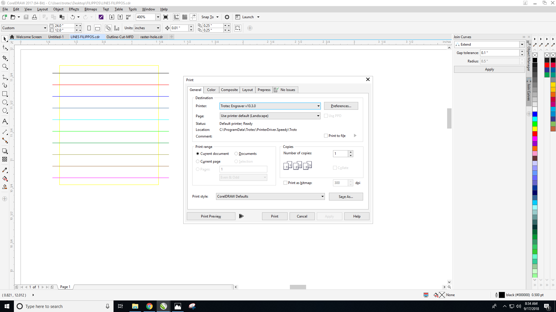
Corel Draw Workflow
Step 1:
Step 2:
Step 3:
Step 4:
Step 5:
Step 6:
Step 7:
Step 8:
Step 9:
Step 10:
Step 11:
Step 12:
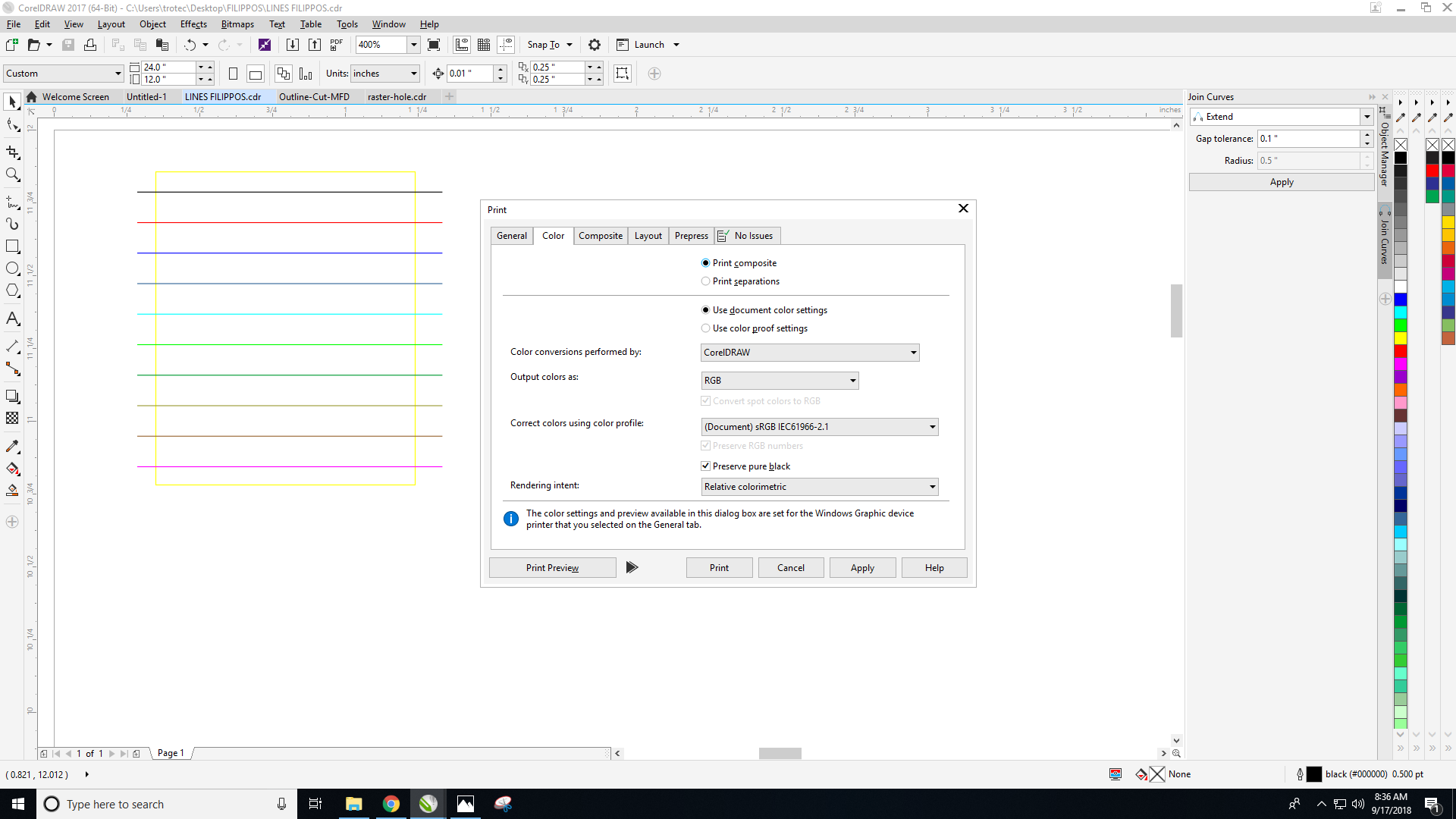
Step 13:
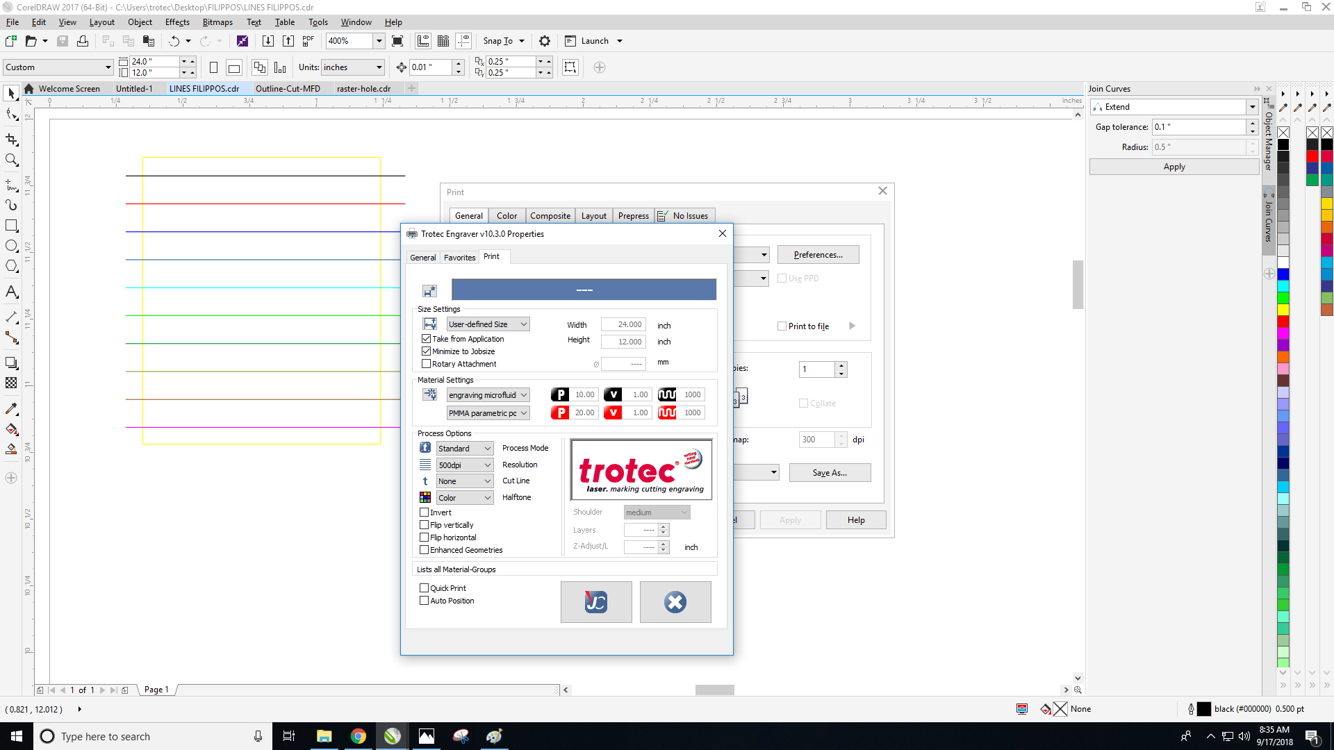
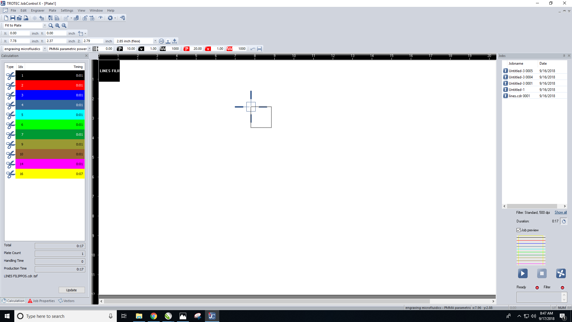
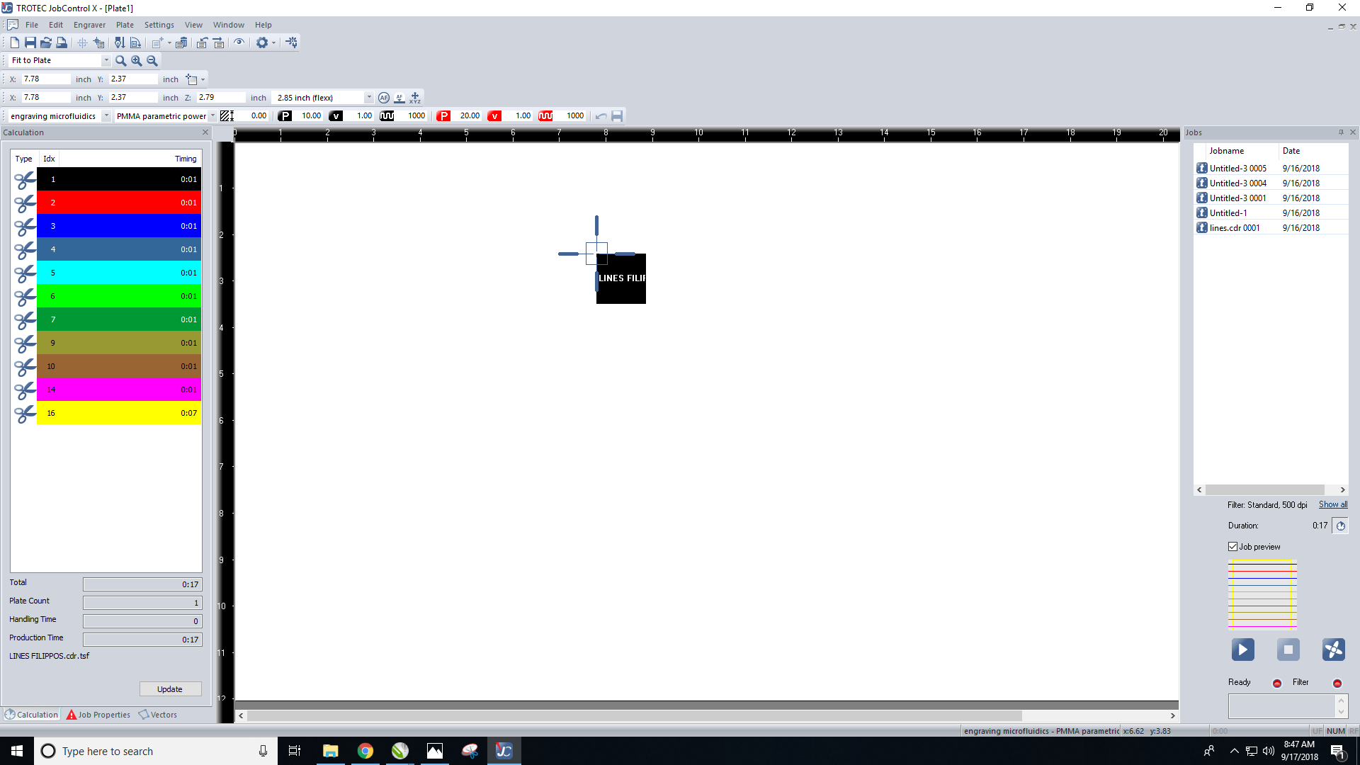
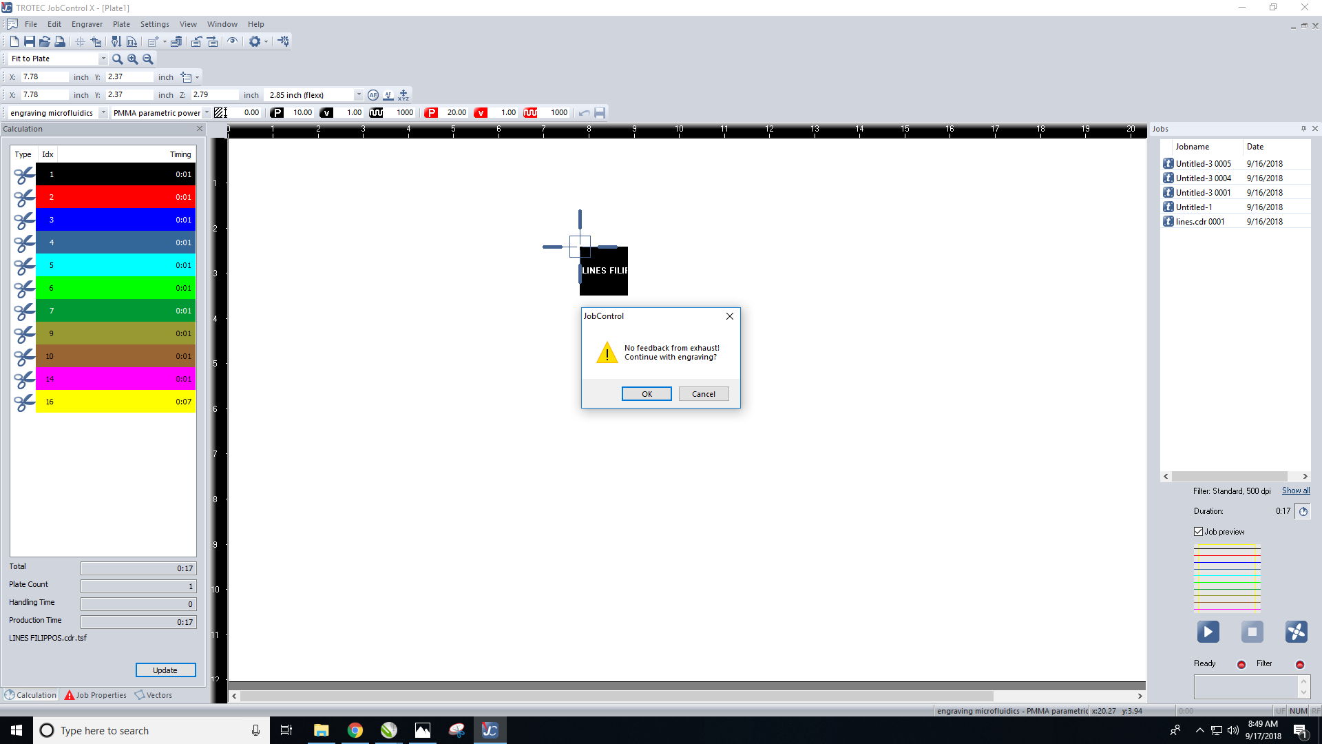
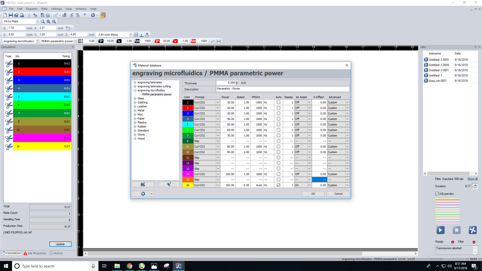
Job Control - Trotec Workflow
Step 1:
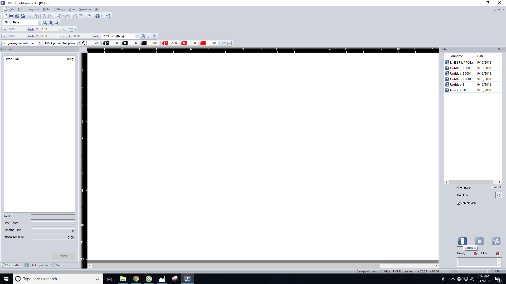
Step 2:
Step 3:

Step 4:
Step 5:
Step 6:
Step 7:

Step 8:

Step 9:

Step 10:
Step 11:
Step 12:
Step 13:

Step 14:
Step 15:

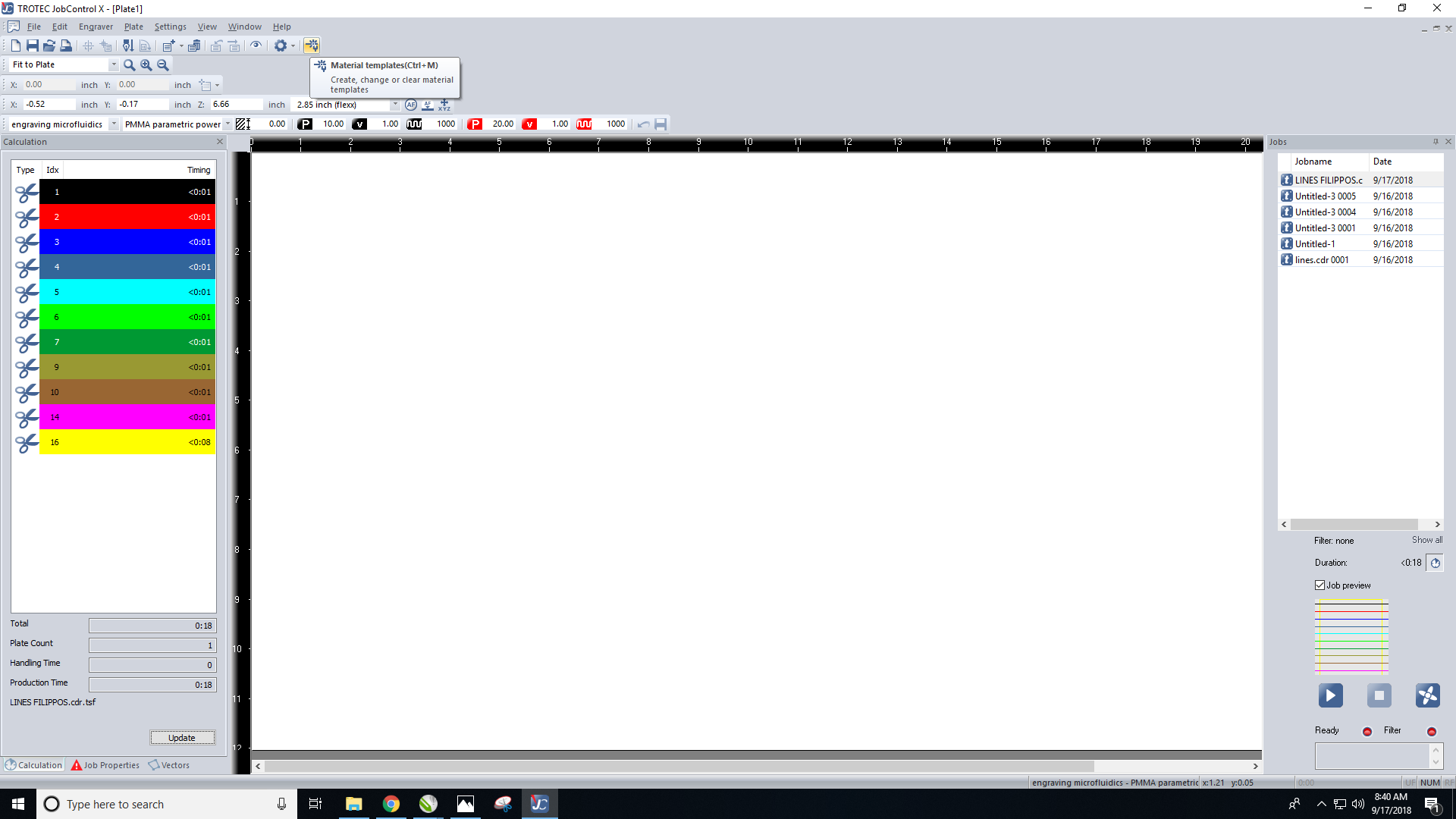
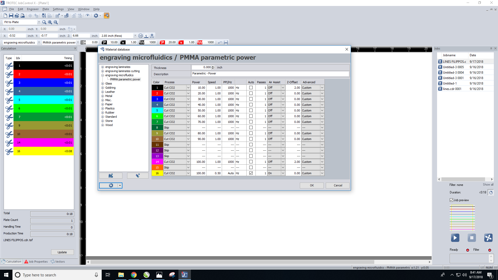
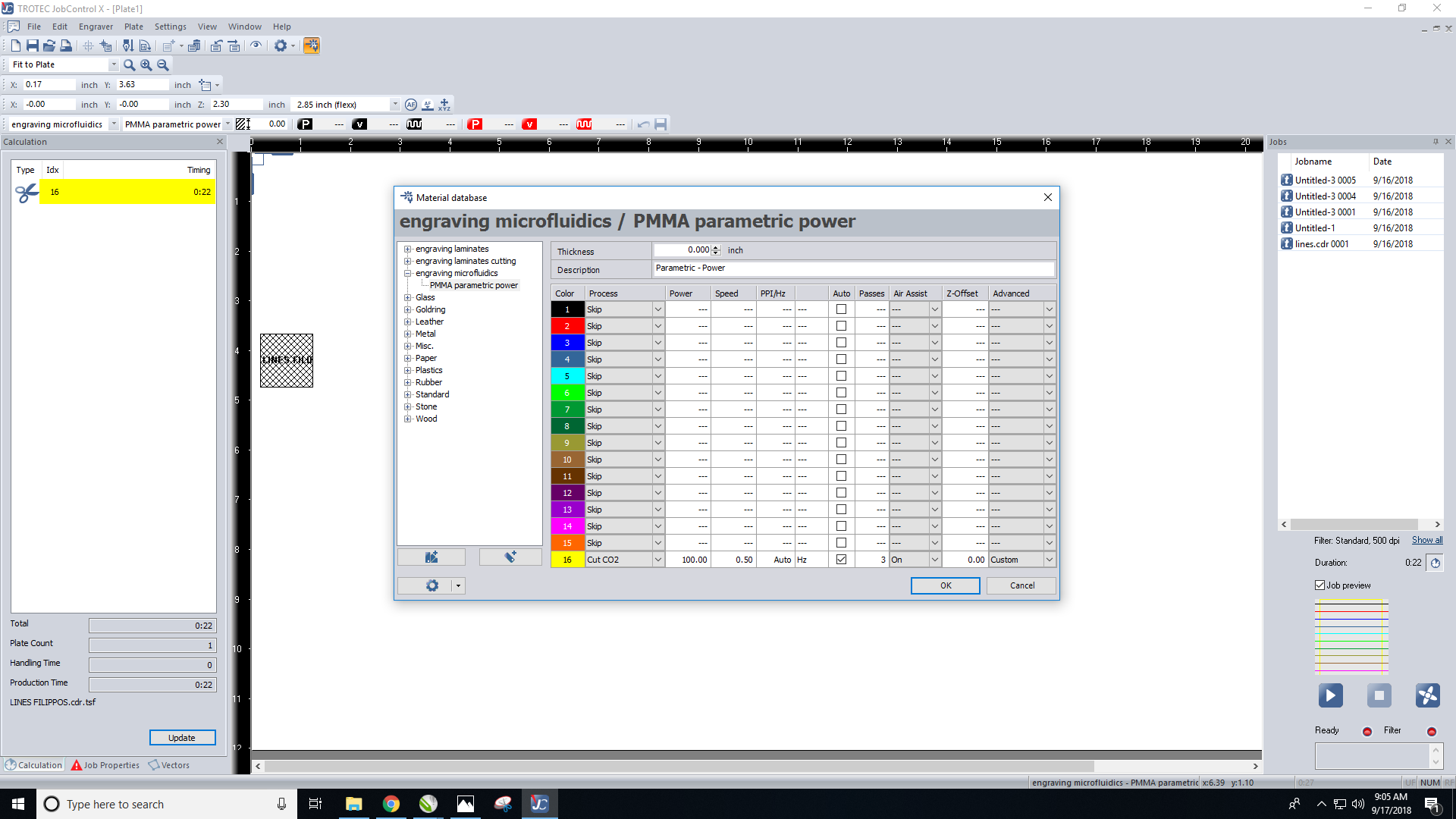
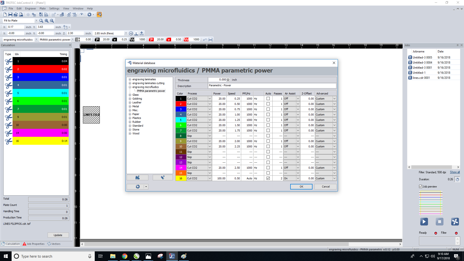
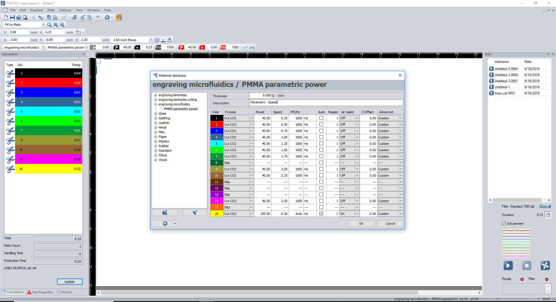
Step 16: Parametric Power Study Settings
Step 17:
Step 18:
Step 19:

Step 20:
Step 21:

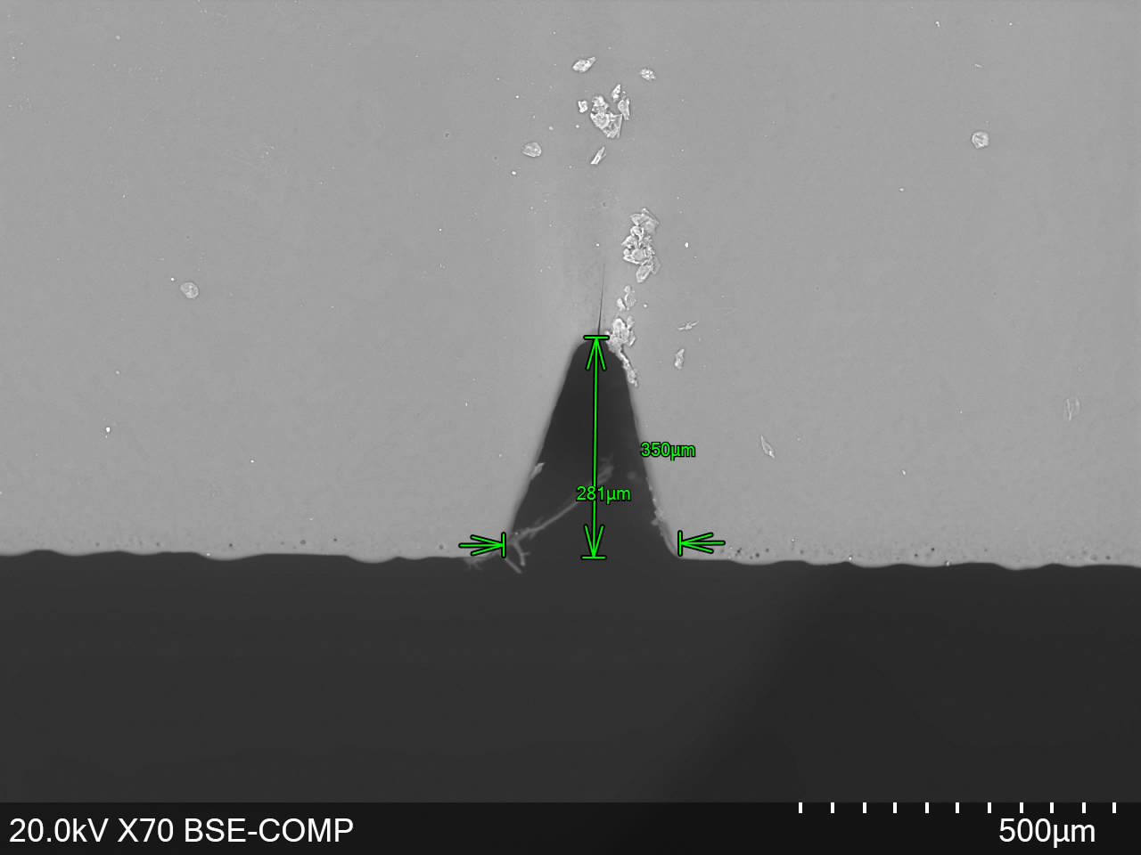
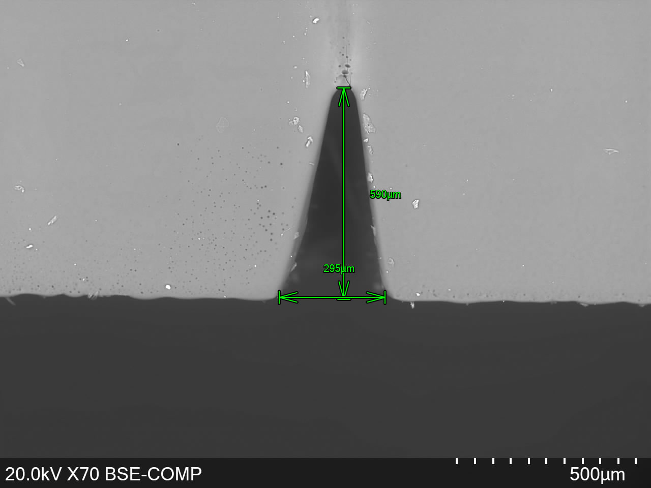
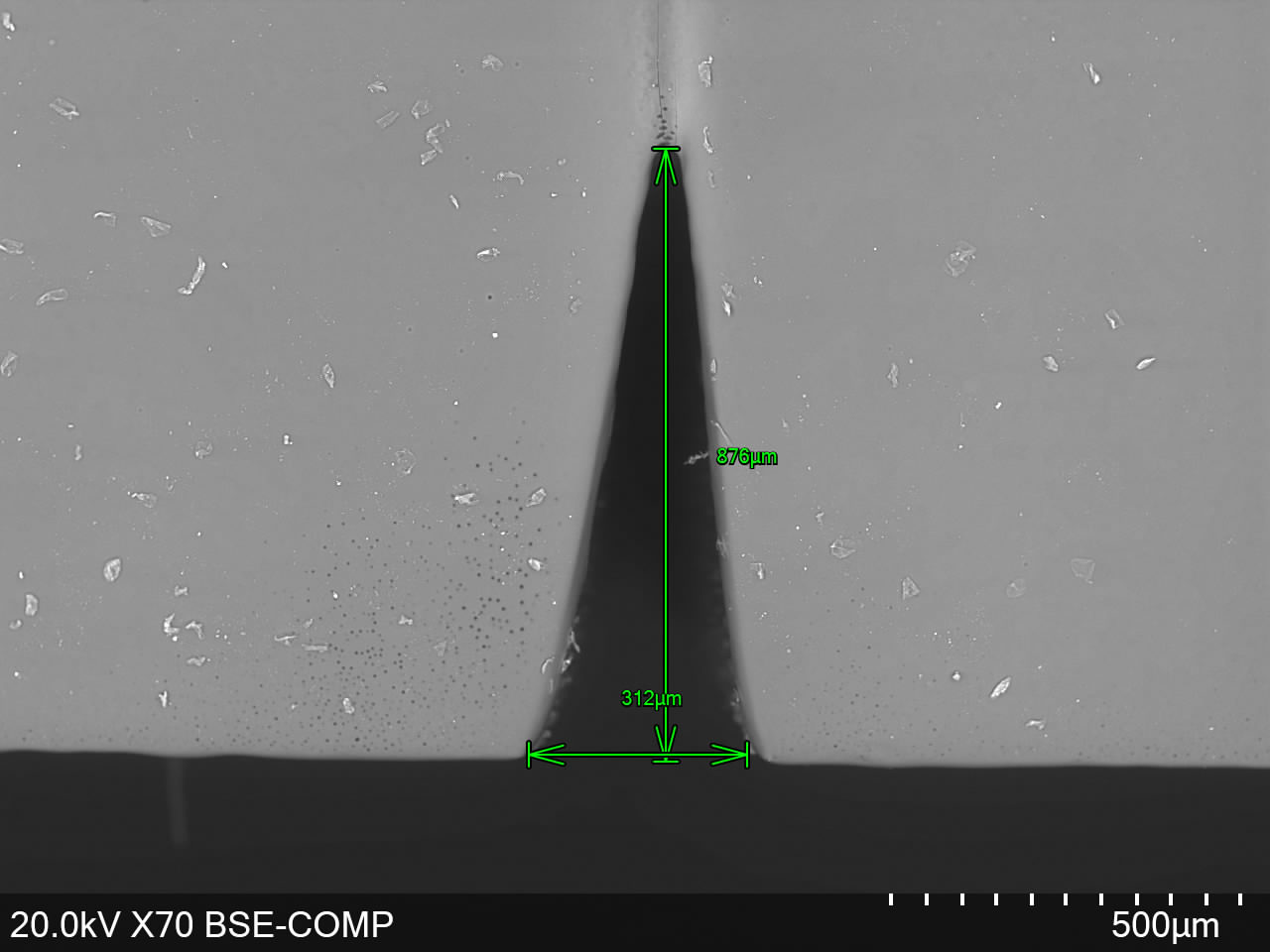
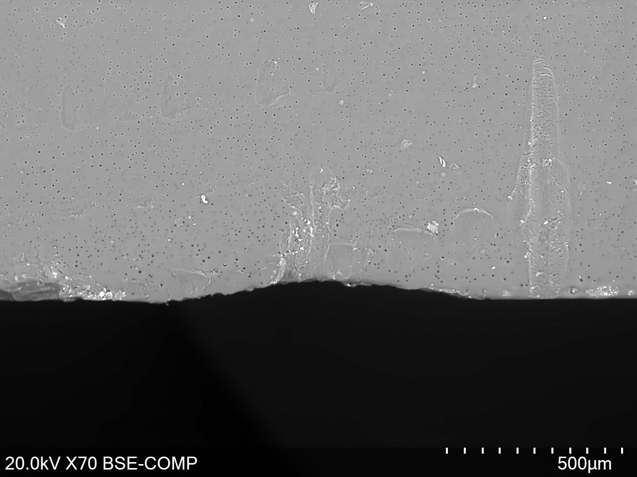
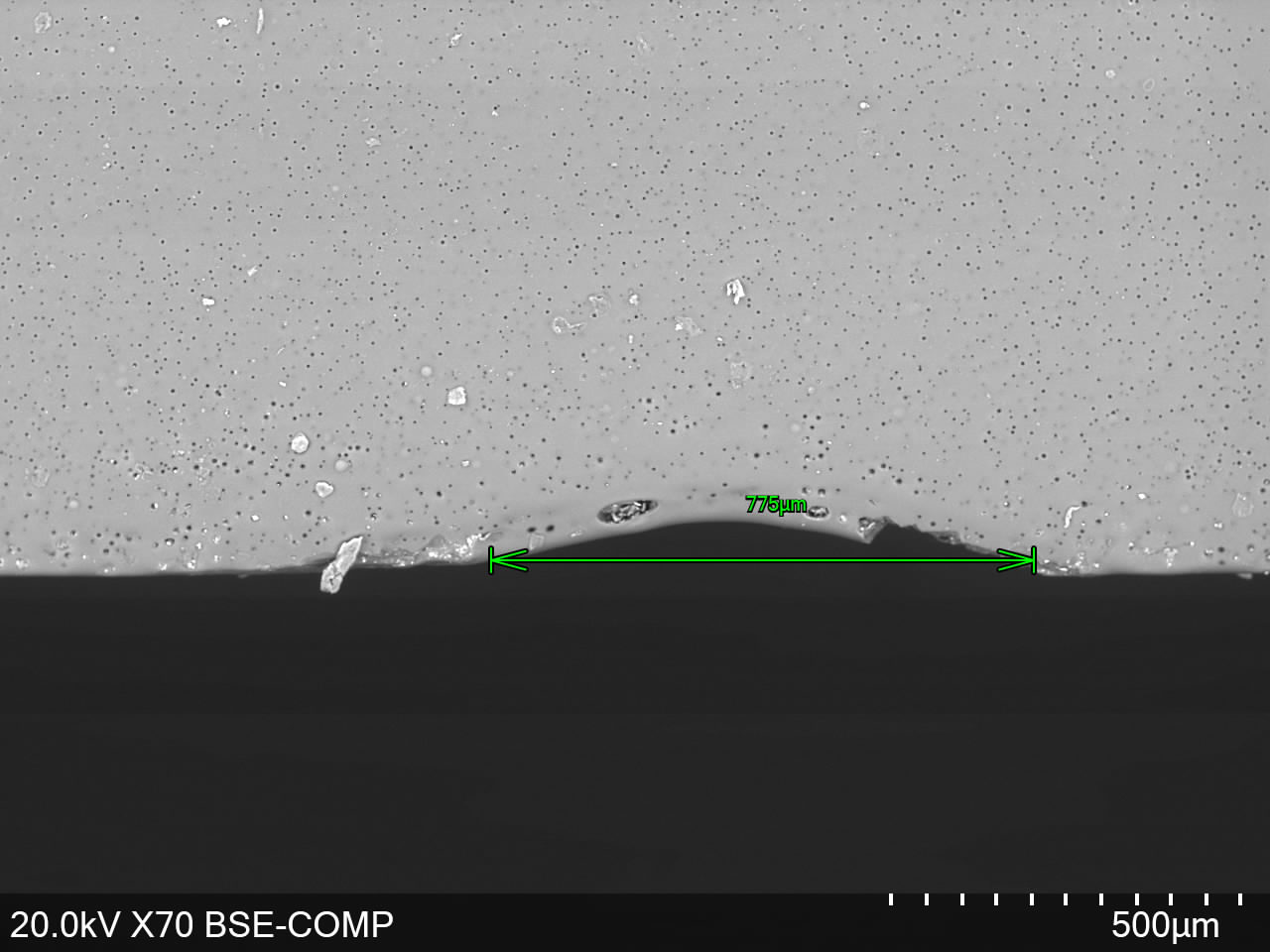
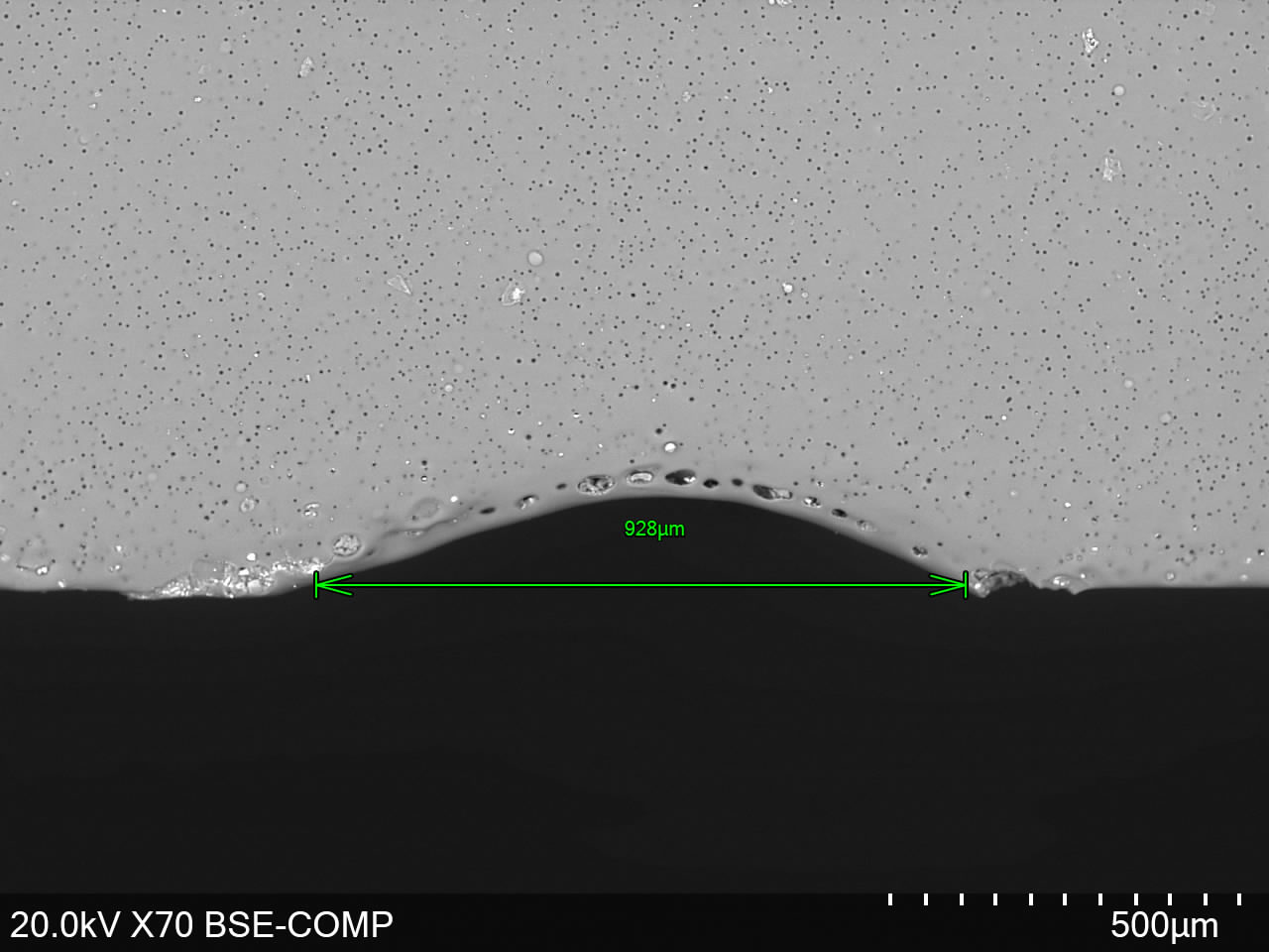
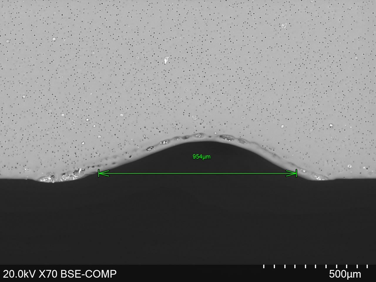
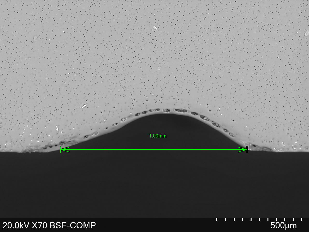
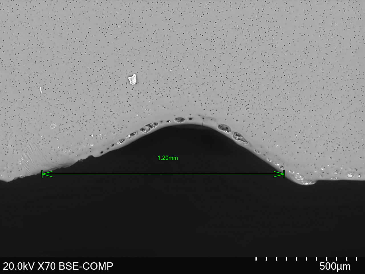
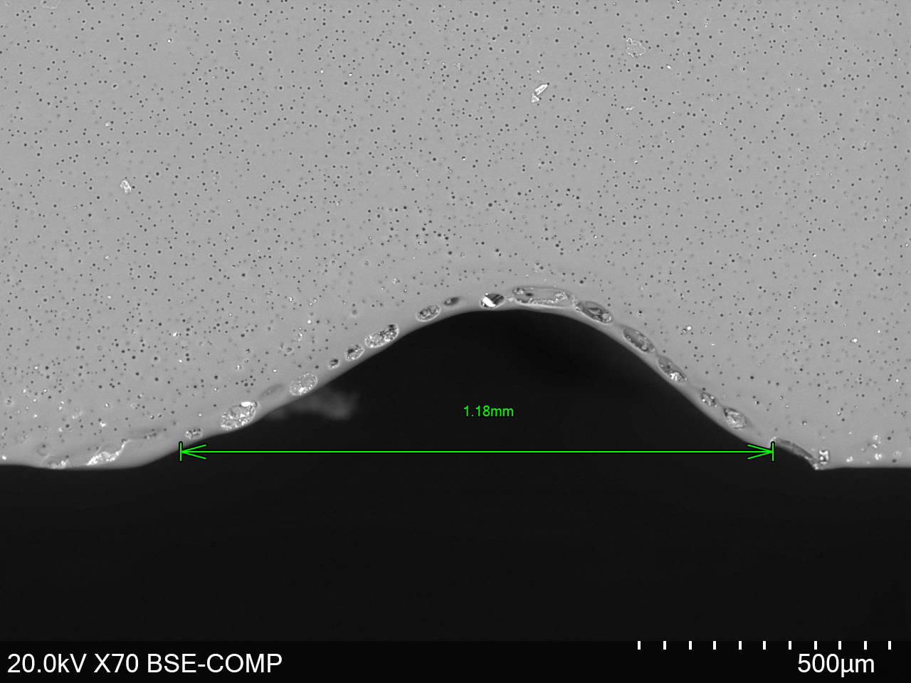
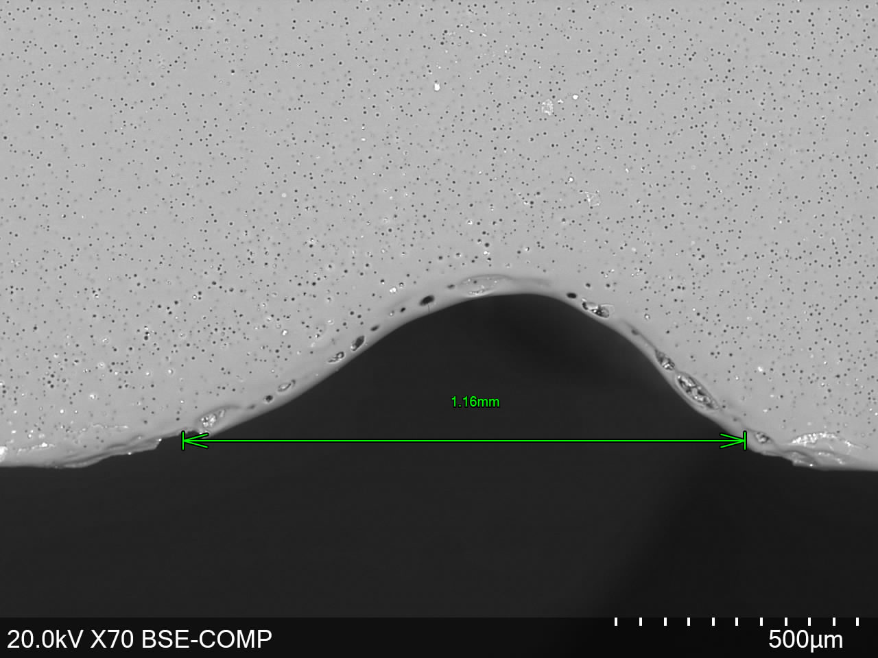
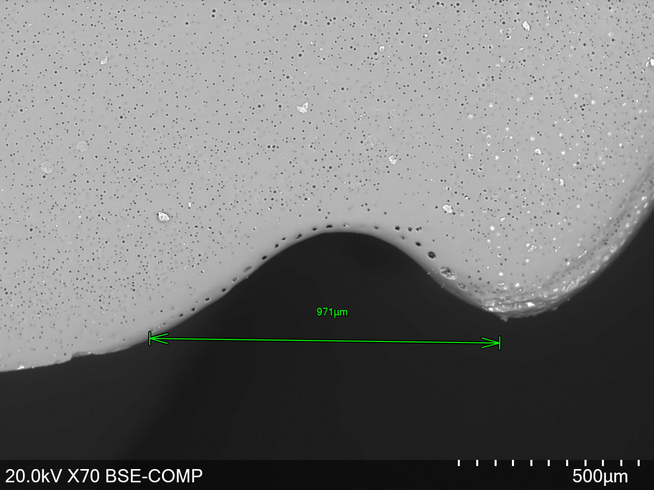
Parametric Studies: Trying to identify combination of process and machine parameters settings for microfluidic channel fabrication.
Change power with a step of 10% (look at Step 17 - Job Control Workflow) an d quantifying laser kerf and channel depth.
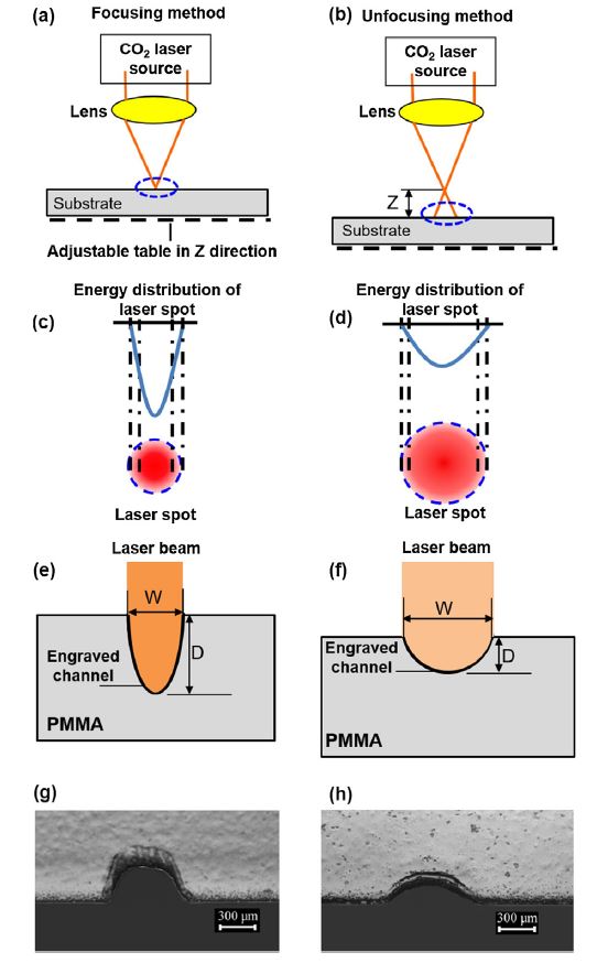
Study 1: Power with Focusing
Power: 10%
Power: 20%
Power: 30%
Power: 40%
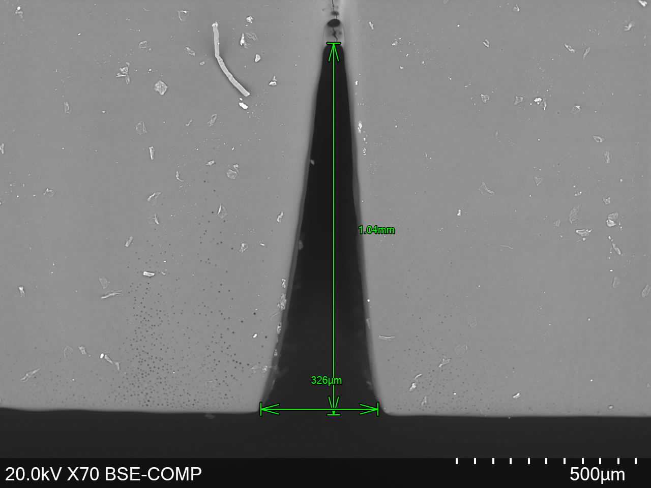
Study 2: Power with De-focusing
Power: 10%
Power: 20%
Power: 30%
Power: 40%
Power: 50%
Power: 60%
Power: 70%
Power: 80%
Power: 90%
Challenges: Assembly-Bonding