Week 13
I’m going to try to reproduce the serial networking example Neil provided because I’m not entirely sure that I’ll be able to work with anything more complicated. I’d like to try wireless communications eventually, but I’m going to try to walk before I run.
I started with Neil’s designs, and because I’m getting more comfortable with KiCAD, I decided to remake them in my own, slightly different design, that includes a power LED, since I like having those. I also have found that I like having rounded edges on my boards, because it somehow makes me think they’re cuter.
I’ve also been fiddling with KiCAD’s design rules settings. I’ve run into issues with overlapping paths in the past, and I wanted to try to reduce the amount of time I spent fixing that. By making some risky connections and testing with mods, I determined that a clearance of 0.4 would reliably make separate traces in the resulting paths. However, on milling the boards, I found that some of the traces were pretty skinny, so I’ll probably bump that up to 0.45 or 0.5 next time I mess around with it.
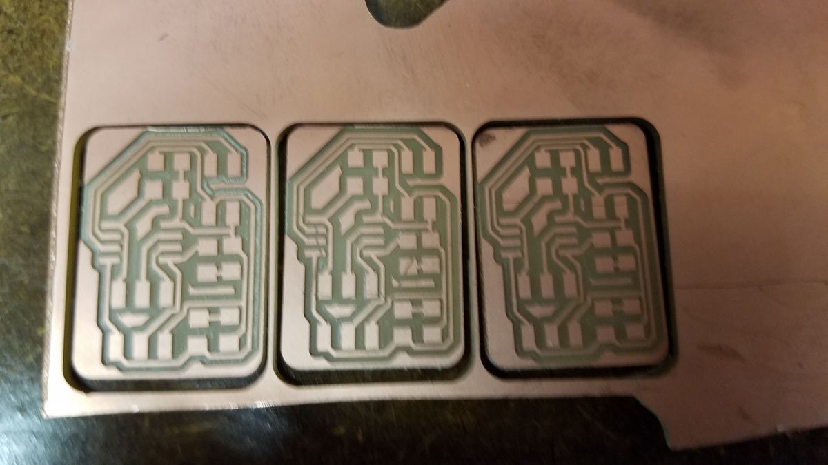
I made the one bridge board in the usual way, exporting an SVG and turning it into a high resolution png. For the node boards, since there are going to be 3 identical boards, I made three copies of the copper and edge traces, then ran convert image1.png image2.png image3.png -append output.png for each set of three to produce three stacked board traces, and then rotated them with mogrify output.png -rotate 90 to change the images in place. That gave me some nicely aligned boards that I was able to mill three at a time.
Here are the CAD files for the milled boards: