Electronics1 Week05
how to make (almost) anything
Electronics Design
Week 05
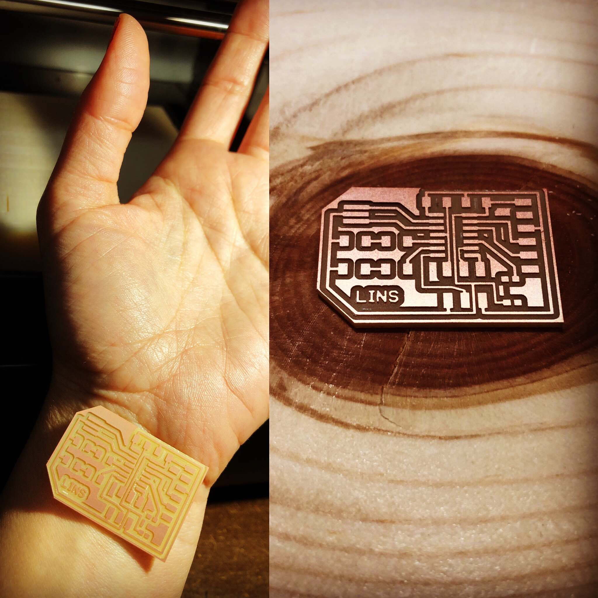
This week’s assignment was to use a computer-aided design software of our choosing in order to re-create the “hello world” PCB. We also had to “stuff it” (solder on the components) as well as program it.
Without prior knowledge of electronics, I began by watching several segments from Barron Stone’s Electronics Foundation course on Lynda. Understanding some of the basics like voltage, current, and resistance along with their systems of measurements and mathematical relationships helped tremendously when decoding Neil’s “hello world” board. Furthermore, getting acquainted with some of the key components like LED’s, resistors, and capacitors along with their schematic symbols made designing the PCB less intimidating. But above all, simply showing up to the lab and relying on the good company of classmates and gurus has been the key to learning what’s most relevant for these class assignments.
At the lab, Rob Hart, our section leader, greatly assisted me in getting rolling with Eagle, a software made specifically for electronics design. After downloading the fab lab Eagle library from Gitlab and dragging it into the Eagle libraries folder, I was able to access and add into my project the components that we have in stock in the lab. (Hint: remember to click on the micro dot beside the “fab” library in the Eagle control panel at the start of each session. It will light up green once activated.) At first glance, the schematic system of labeling and spatial orientation of parts is confounding. I am grateful for Rob’s patience and generosity in helping me make sense of it all.
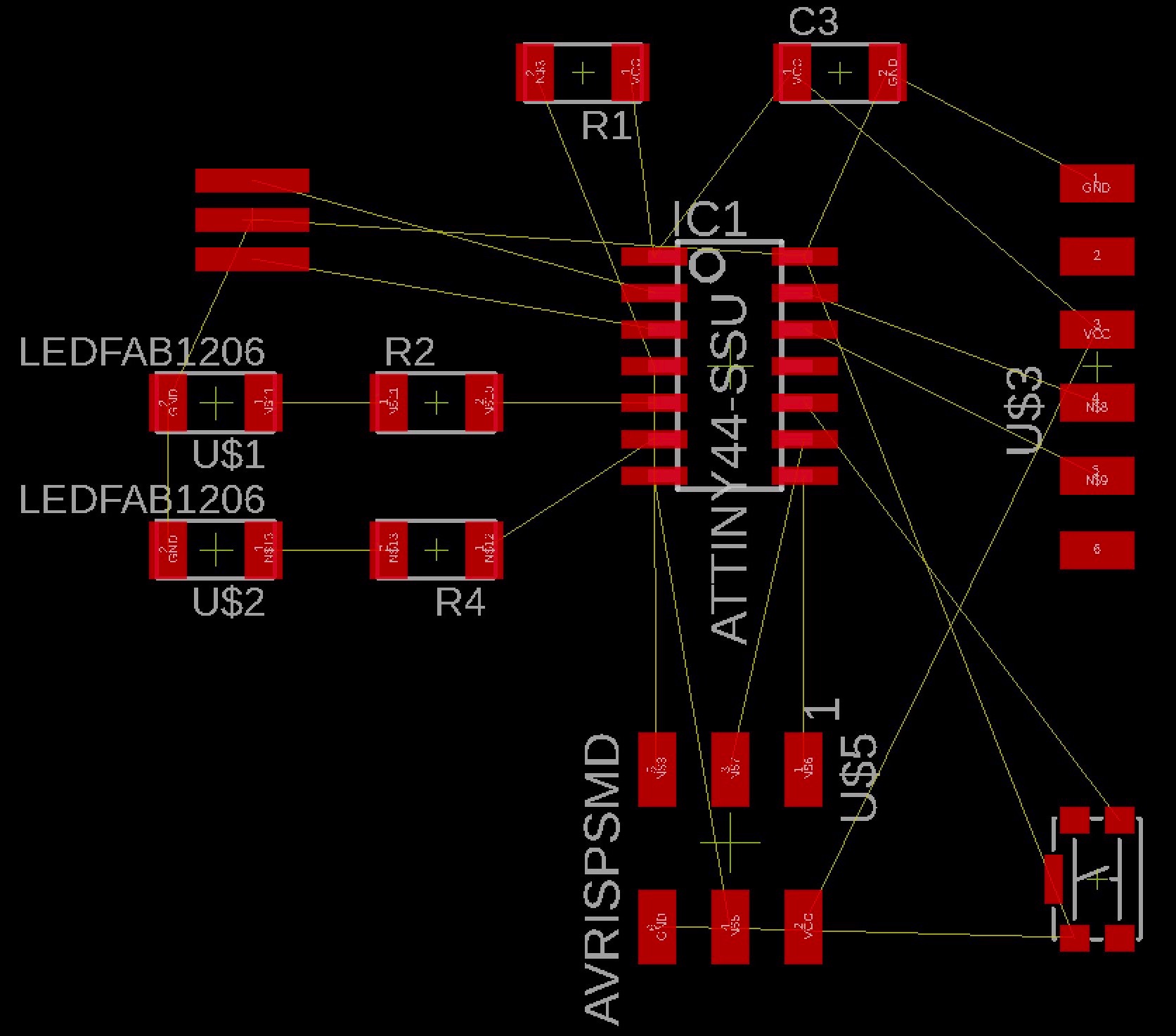
Simply explained, in the schematic, add the parts you need for your project then draw lines between the parts to indicate their connections or wiring. Once in the board view, you must then decide where each part will go then convert those schematic lines into traces for the milling machine to follow.
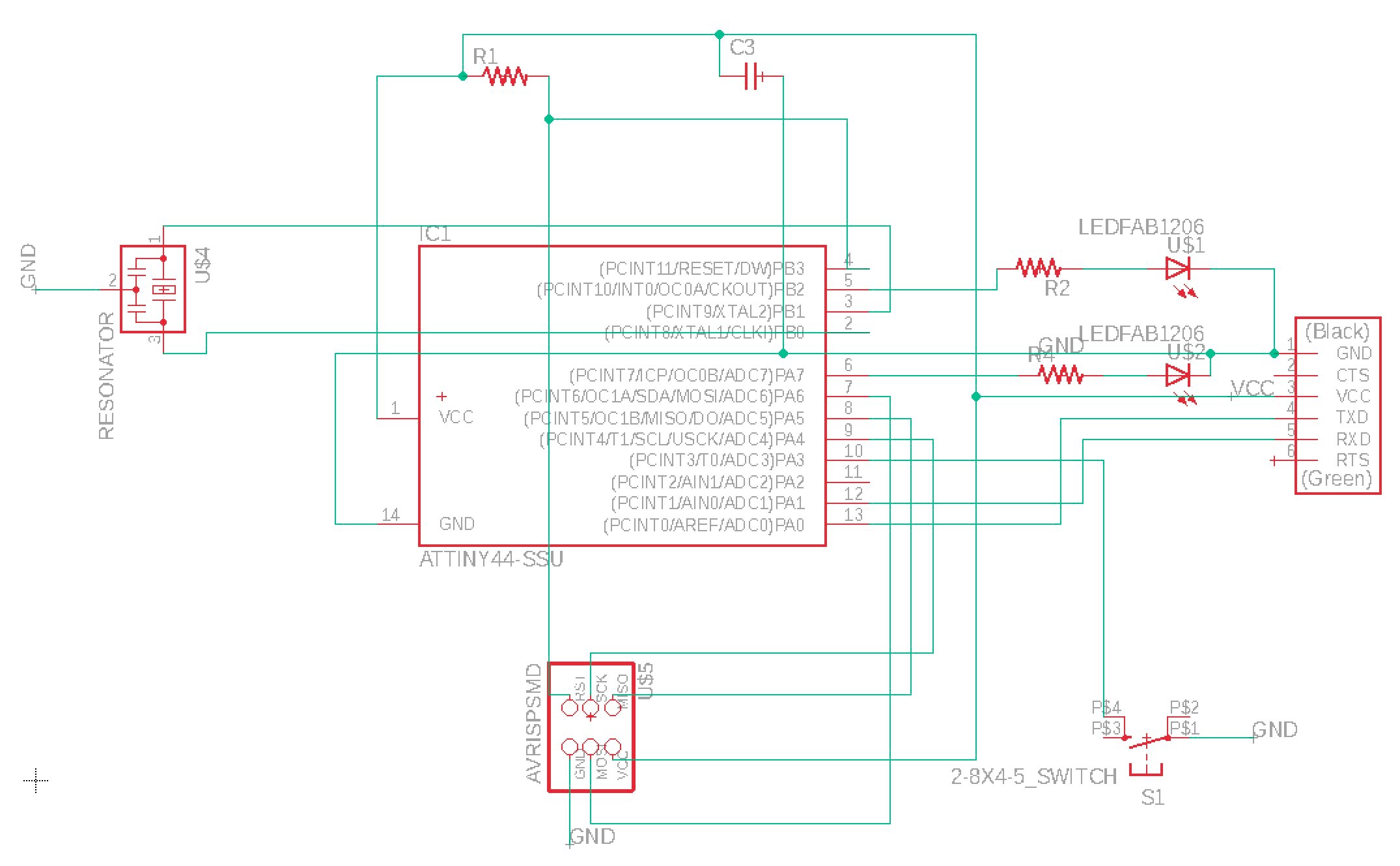
At first, the schematic lines looked like a rat’s nest, just as they are officially referred to, but as I began to use the trace tool to make the connections between components, I saw how helpful they were. They are like pencil lines, keeping track of your original schematic sketch as you make design decisions about the paths of each trace. Unfortunately, even using the auto setting that enforced the PCB design rules as well as the DRC check for hidden errors, I still had to adjust my design several times during the milling process.
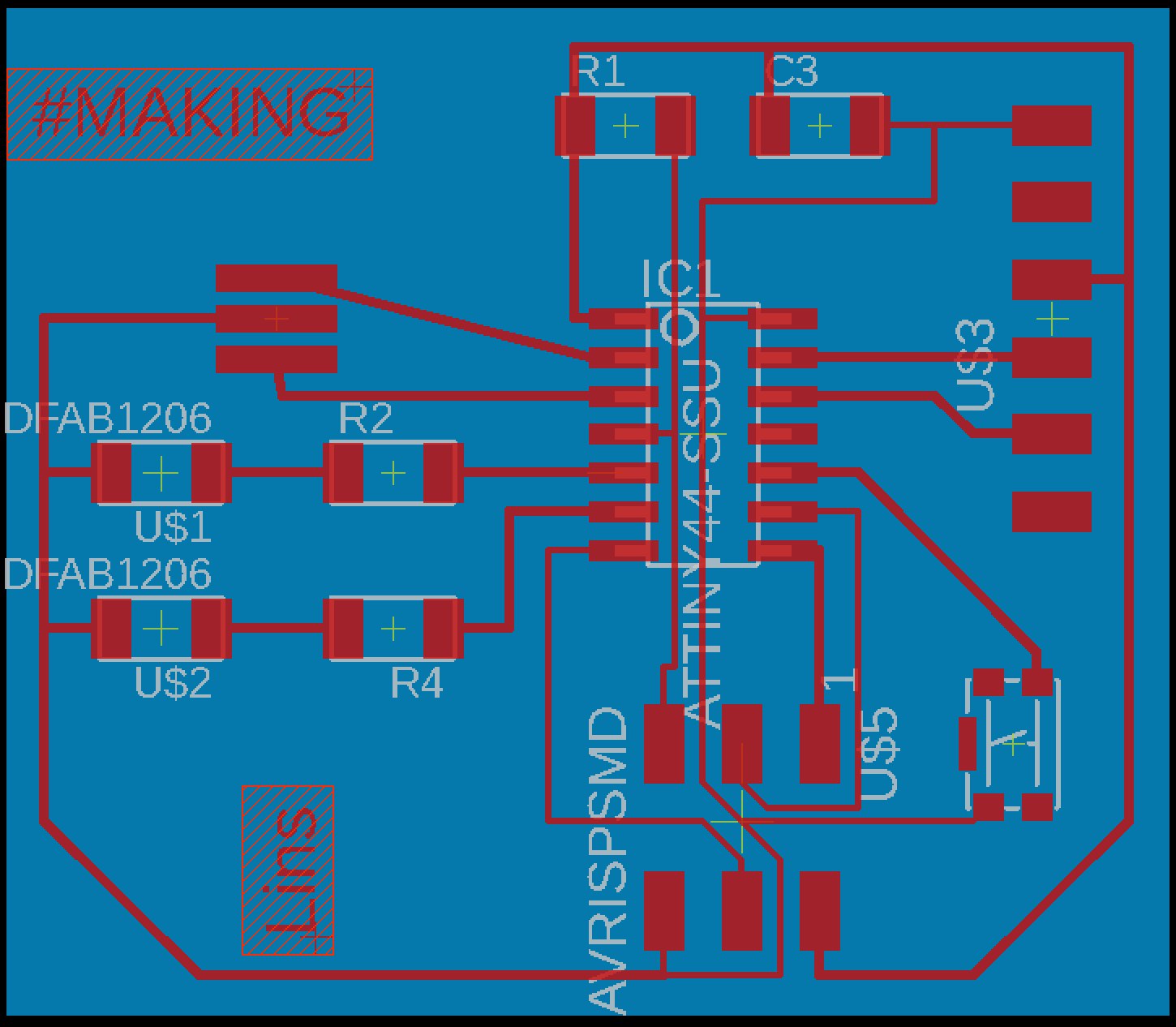
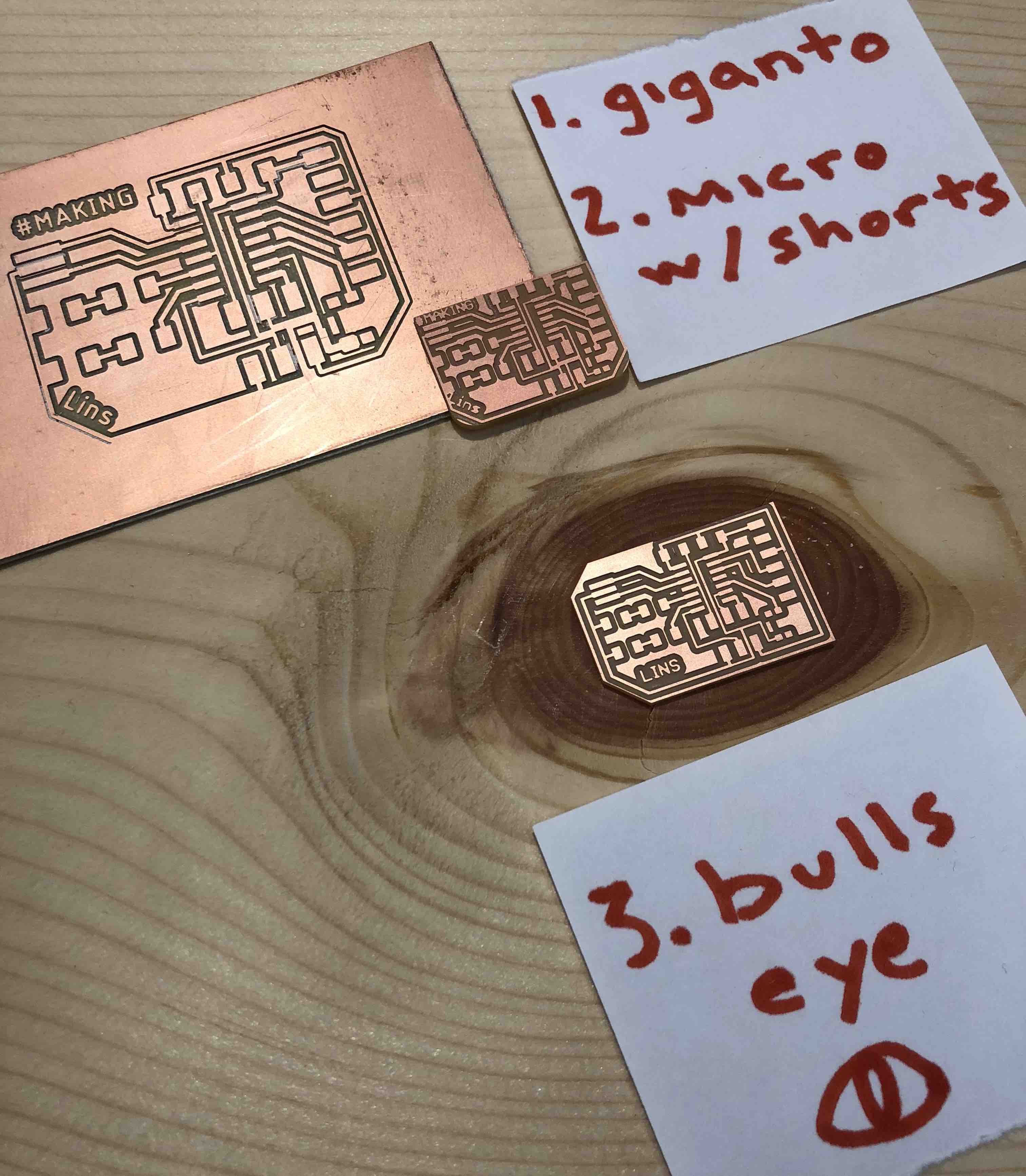
In quick summary, the new MacBook Pro’s do not export .brd to .png well. Below examples were both exported at 1,000 dpi but the Mac version came out super-sized as compared to the Window’s one. Once I figured this out, I still had to edit my design because of traces unintentionally merging and shorting in certain areas.
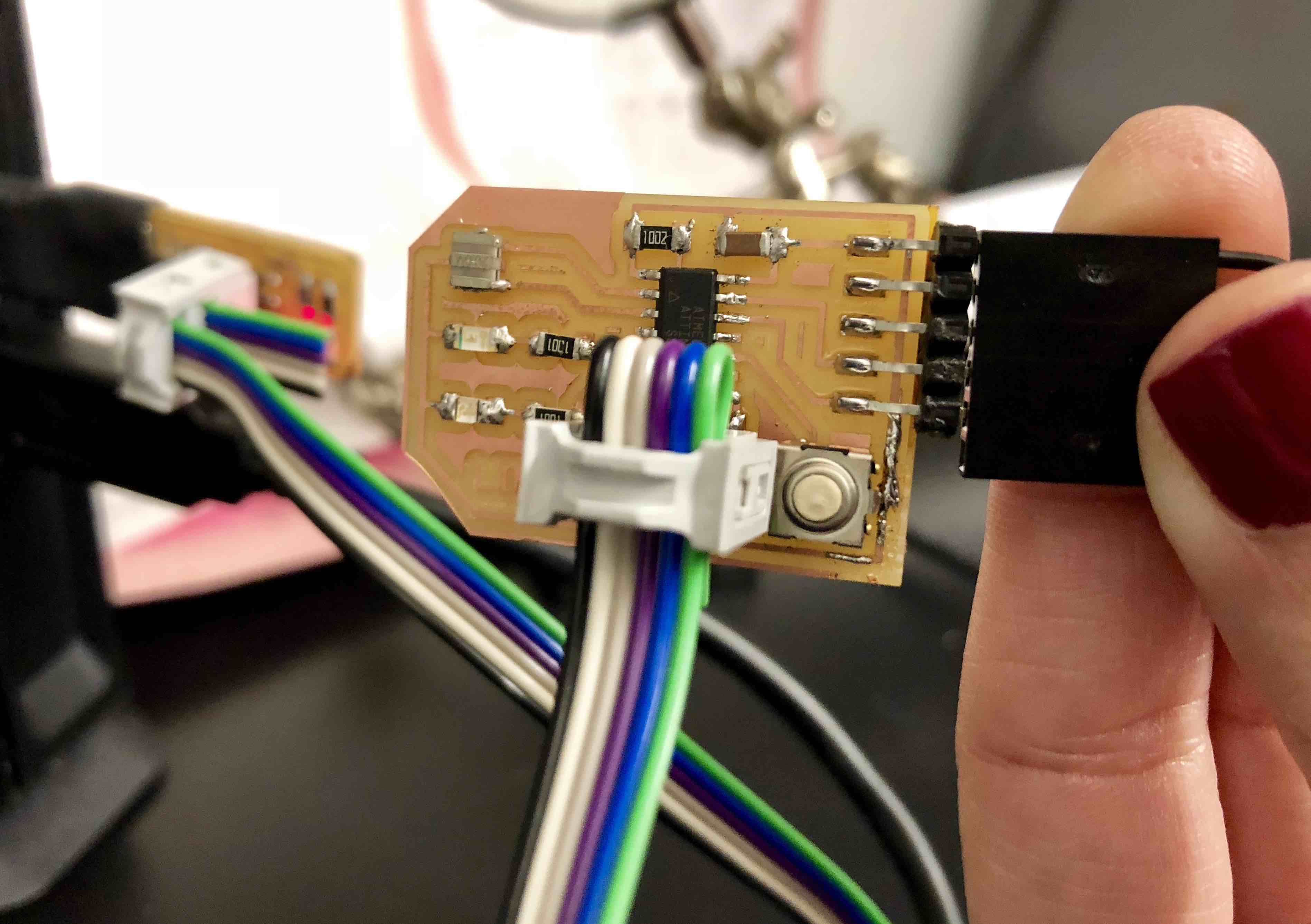
Soldering remains a tedious and patient ordeal even after the practice had in the Electronics Production week. While I lost my touch as quickly as I had gained it, I did, however, find a new tactic for soldering on multi-pronged components such as the Attiny44: the hot air gun. Here’s the method…
Dab solder on all the copper pads for the component. Since solder hardens immediately, hot air blast the newly coated pads till shinny. Adhere the component with tweezers all at once. This tactic beats soldering one end or peg down at a time, although I question the long term effects of hot air blasting the entire board and nearby plastic components repeatedly.
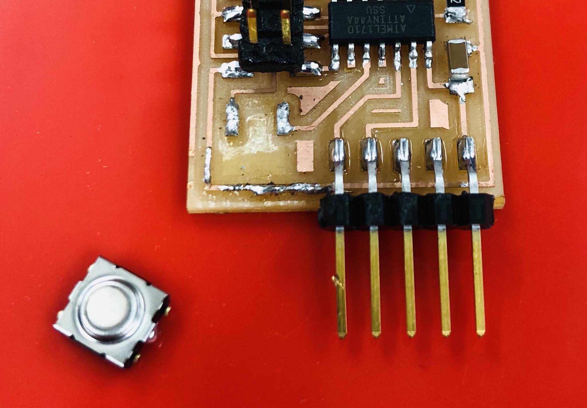
Not surprising, mistakes made in my Eagle design that went undetected during milling became apparent during the soldering phase. In Eagle via the fab library, I selected the incorrect “button” which printed pads way too small for the actual component. Fortunately, I was able to jury rig it by using an XACTO knife to remove the copper pads which were placed too tightly together in order to prevent the circuit from shorting. Of course, I left the essential copper pads on to make the button work. Overall, this process was far from ideal as I snagged the VCC (power) outer trace with the XACTO and had to repair it using a wire bridge after. The odds for placing the Attiny44 in the right orientation are 1:2. This worked in my favor since I forgot to check my Eagle schematic when soldering on this part. (Look for the “dot”!) And just so I keep it straight next time, I used:
- 5-legged power plug
- 2x3
- Attiny44
- Resonator
- Switch or “button”
- 1MF capacitor
- 10k ohms resistor for the one connected to the Attiny44 reset and 2x3 reset ports
- Two LEDs with two corresponding 1k ohms resistors
As for the programming between Week 03’s programmer and this week’s PCB, I used the computer in the Harvard Science Lab which already had the hello-world file on the desktop and text editor up. I followed religiously guru Julia’s directions that she posted last year when she took the class. Thank you Julia!
Here’s the link:
http://fab.cba.mit.edu/classes/863.17/Harvard/people/julia-ebert/2017/10/04/electronics-design.html