WEEK05: electronics design
 This week we learned the basics of electronic circuit design. The lecture was a crash course in EE basics: Kirchoff's laws, electronic design tools, Ohm's law, circuit routing, schematics, and the rest. I have experience in this world, so I held office hours opposite Jake; he taught folks Eagle, while I showed them how to use KiCad.
Our assignments were twofold: (a) recreate the Hello World board discussed in the Week 3 lecture, which uses an ATtiny44 to echo charcters over a bit-banged UART connectoin; and (b) use the lab instruments to characterize our devices.
This week we learned the basics of electronic circuit design. The lecture was a crash course in EE basics: Kirchoff's laws, electronic design tools, Ohm's law, circuit routing, schematics, and the rest. I have experience in this world, so I held office hours opposite Jake; he taught folks Eagle, while I showed them how to use KiCad.
Our assignments were twofold: (a) recreate the Hello World board discussed in the Week 3 lecture, which uses an ATtiny44 to echo charcters over a bit-banged UART connectoin; and (b) use the lab instruments to characterize our devices.
files
- Hello World KiCad PCB files and firmware
hello world, pcb edition
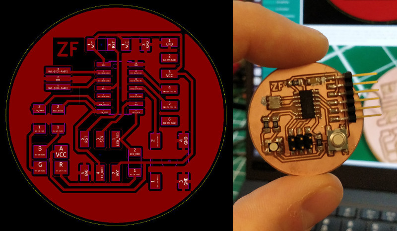
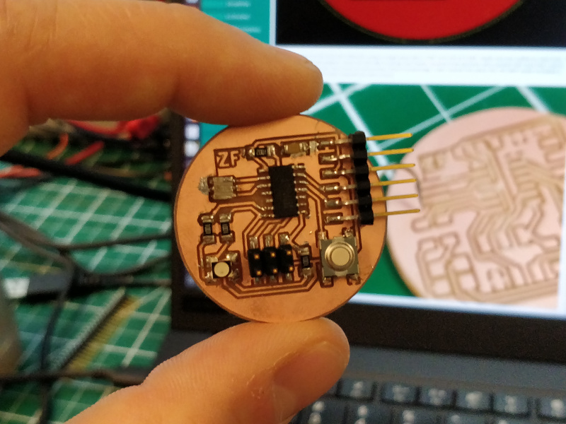
I used KiCad, an open-source EDA tool supported by CERN, to recreate the Hello World board. First, I drew a schematic, adding a switch and an RGB LED with a few current-limiting resistors. I decided to use labels rather than drawing all the wires to keep the schematic clean: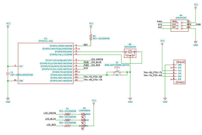 Keen observers will notice that I labeled MOSI and MISO with PORI and PIRO: Primary Out, Replicant In; Primary In, Replicant Out. I'm not convinced these particular terms will stick, but I do think it's worthwhile to stop using the language of slavery when describing electronic communication wiring.
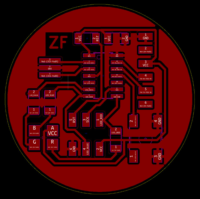
After cloning the fab KiCad libraries and assigning footprints, I set my design rules to 0.4 mm / 0.4 mm and routed a circular single-sided board with a ground pour that uses the momentary switch to jump over a track, thus avoiding the need for vias:
Keen observers will notice that I labeled MOSI and MISO with PORI and PIRO: Primary Out, Replicant In; Primary In, Replicant Out. I'm not convinced these particular terms will stick, but I do think it's worthwhile to stop using the language of slavery when describing electronic communication wiring.
After cloning the fab KiCad libraries and assigning footprints, I set my design rules to 0.4 mm / 0.4 mm and routed a circular single-sided board with a ground pour that uses the momentary switch to jump over a track, thus avoiding the need for vias:
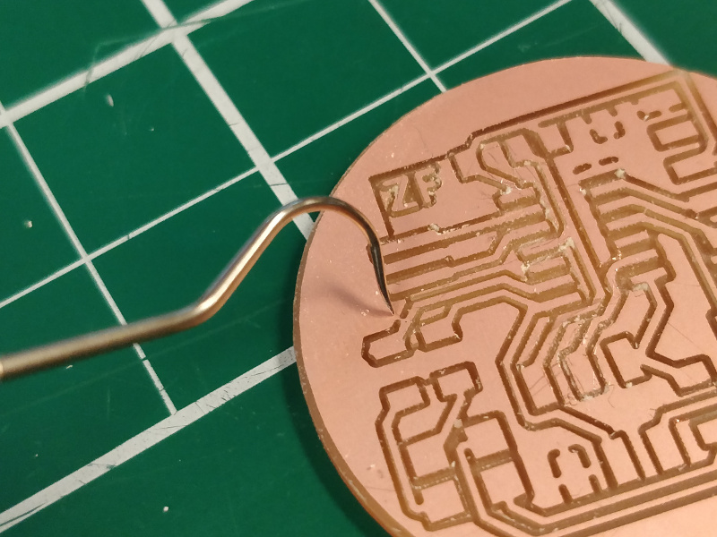
 I routed the board on the E15-023 SRM-20, using a single pass with a 1/64" end mill at 0.004" depth and one outline to save time. This created an unexpected problem: since the mill didn't overlap any traces, several of the grooves were packed with dust that I had to pick out using a dental tool. Not much of a time-saver. More concerningly, I also noticed one place the mill didn't quite complete a route, creating a tiny short that I cleaned out with a razor:
 I modified the original firmware slightly to toggle the RGB LED color with every echoed character, programmed the board using the hand-carved programmer from Week 03, and gave it a test using gtkterm and a USB-serial cable:
[command: ffmpeg -i VID_20191008_181749.mp4 -filter:v "scale=800:-1" -ss 00:00:00.0 -t 00:00:05.0 -c:a copy out.mp4]
okay now make a tiny one
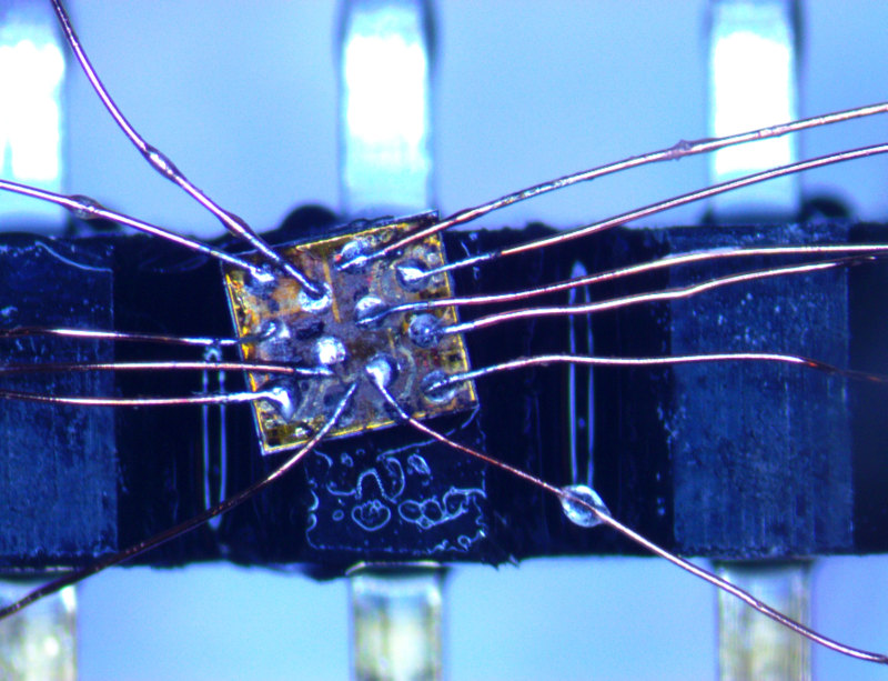
I decided to make another version of the echo board using the smallest components I could. This involved using the smallest ATtiny available: the 1.5 mm x 1.5 mm wafer-level chip scale package ATtiny20: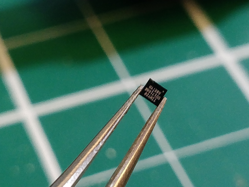 This chip is well outside the realm of PCB milling, even with a 0.010" mill, so I used a microscope, a fine iron tip, plenty of flux, and 42 AWG polyurethane insulated copper wire to dead-bug it to the 1x6 FTDI header:
 All seemed well; I hooked the wires up to larger wires, and then up to my programmer. But I wasn't able to flash the chip; turns out the ATtiny20 and other small devices in the series use a specific programming protocol called TWI, which is distinct from the ISP that my programmer supports. Bummer. This goes back on the shelf for future investigation.
device characterization
One interesting test is to measure how long it takes the ATtiny44 to process an incoming UART character and send a response. I used the MDO3024 at my desk in E15-023 for this purpose. Wiring was simple enough; one probe on each of the TX and RX lines, and a ground clipped to the PCB plane: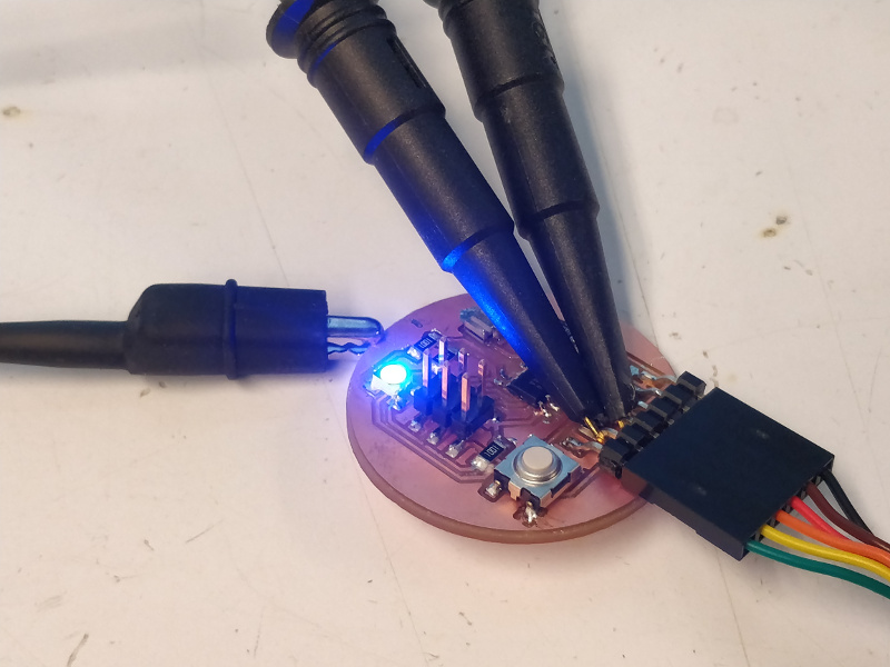 I typed the character "U", which is a good sample because its waveform shows up at a square wave with four peaks and five valleys. The first eight bits (01010101) are the binary code for the ASCII letter "U", while the last low bit is the parity bit. By measuring the time between this last bit going high (yellow trace) and the first response from the ATtiny44 (blue trace), we can quantify the processor's echo speed:
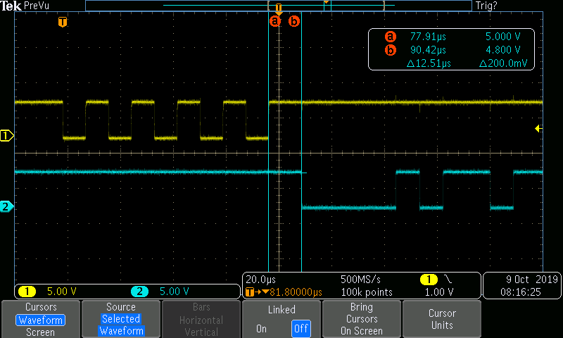 The inset window shows the time differential between the two cursor lines: 12.51 us. Given the speed of sound in air at 20 degrees C of 343 m/s, this suggest the ATtiny44 circuit responds at the same rate as the echo from screaming at a wall ~2mm in front of one's face.