Designing my Custom Hello World Circuit
Understanding the Microcontroller
Two weeks ago, we had been provided the board design (in PNG) that we were supposed to make. Thus, the process had pretty much been milling the provided board, soldering the components on the milled board based on the instructions provided and programming the board, again based on step by step instructions provided to us. I did not take the time to understand why the components were configured in a particular way. I did not understand the different pins of the microcontroller and their functionality. This week though, I decided to learn a little about it. I spent a few hours learning about microcontroller, different protocols of communication with the microcontrollers used and so on. I still have a lot more to learn, however for this week I believe I can now go ahead and design my own working circuit.
Circuit Schematic Design
I looked at the Hello World circuit designed by Neil. The only thing that was accesible was the board layout. Just based on that, it was hard to tell which components were laid out on the board exactly. After some trial and error I figured it out what components were there. I drew a rough schematic of the board on paper. I then decided to use Eagle for rest of the desgin. I had never used Eagle before, just like so many other software I have to use in this class. I found a Youtube tutorial about Eagle which explained in great detail how to get started with it. Before starting my own schematic in Eagle, I added the FAB library to Eagle. Then, I began my schematic. I replicated Neil's Hello World circuit in the schematic. In addition to the "Hello World" circuit, I had to add an LED and a switch at minimum to the circuit. Since, all of this was already so new and overwhelming to me, I decided to make a very simple addition to the "Hello World" circuit's schematic: a series circuit of an LED, a resistor and a switch connecting VCC to GND.
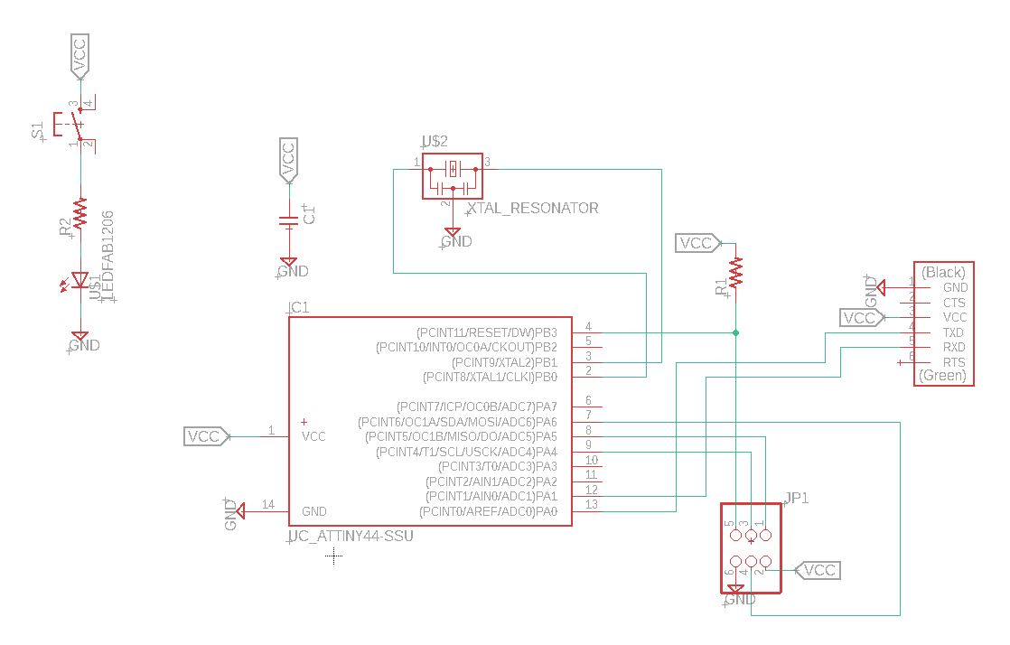 Schematic of Circuit
Circuit Board Design and Routing
Using Eagle's "Generate Board" tool, I generated a raw board with all the components and the nets (wire connections). My next task was to arrange the components on the board well to minimize routing issues later on. Since I had not arranged components or done net routing before, I stuck to making my board 1 layered. Making it 2 layered would involve complicated routing. Arranging components can be challenging if there are multiple components. Luckily, Neil's "Hello World" board again shed light on this. I arranged all the components of the original "Hello World" circuit just like Neil had done. I just had to arrange my switch, resistor and LED which was relatively easy. Next step was routing. I had wanted to do auto-routing, however, Harrison advised me against it. He just taught me to do manual routing, and I just fell in love with it. There was something fun about drawing the routes. I got done with routing on Monday around 7:30, but the lab closed then, so I could not mill my board.
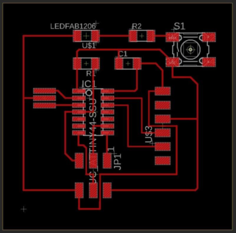 Designing the Board
Failure (Learning) On First Attempt
When you try, you either succeed or you learn. It's only an failure when you do not try. - Unknown Source
On Tuesday, I went to lab with my routed board design. I exported the inline and the outlines into PNG and started milling using the SRM-20. I had forgotten how to use the SRM-20 for milling, so I had to re-learn it. Nevertheless, once the machine got going, I felt a sense of excitement. After 15 minutes, I took out the milled board and the board did not look too good, the outline had almost overlapped with the inlines, the traces seemed too thin and upon further inspection I realized the line traces had merged with components and it was a failed milling attempt. I went back to my board design and figured the problem was, the routed nets were very close to the component traces.
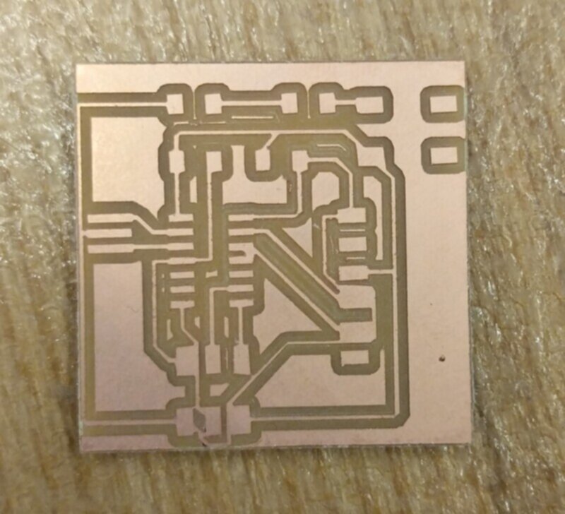 Bad Mill
Fixing the Routing and Second Mill
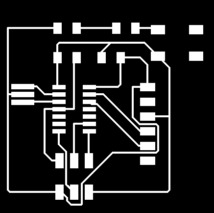
I re-did a lot of the routings since they were close enough to the component traces that they might come out merged after the milling. I also changed the thickness of the wires from 12 to 10 in places where they might merge with component traces. After re-routing, I went to mill my board again. This time however, I used the "Other Mill", not the SRM-20. The "Other Mill" was much easier to use and also much smarter compared to the SRM-20. I did not have to adjst the axes for the mill or anything. I started the mill and had my fingers crossed as the milling worked. What came out was a beautiful board. The outline was much further out, the traces had separated well, no traces looked like they would come off, it just looked so much better than the first time.
 First Attempt at Routing
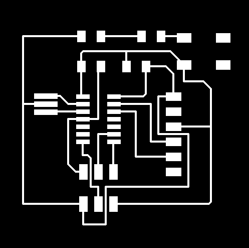 Re-Routed
Soldering and Programming
I gathered all the components and started soldering. I used the solder paste this time to solder some big components. The solder paste was so much more efficient than soldering by hand. It was super neat as well. Soldering felt easier and fun this time around. After soldering, I needed to program my board. Programming was not too difficult. Since I did not have any programmable logic associated with the LED or switch I had added, I just programmed the way Niel's "Hello World" circuit had been programmed. I got the echo of the letters from my circuit and that implied, everything was working!
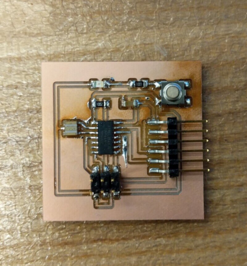 Soldered Board
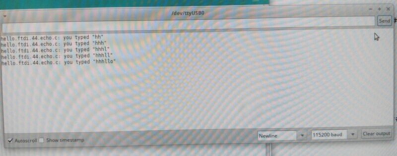 Successful Echo