Week 3: Electronics Production
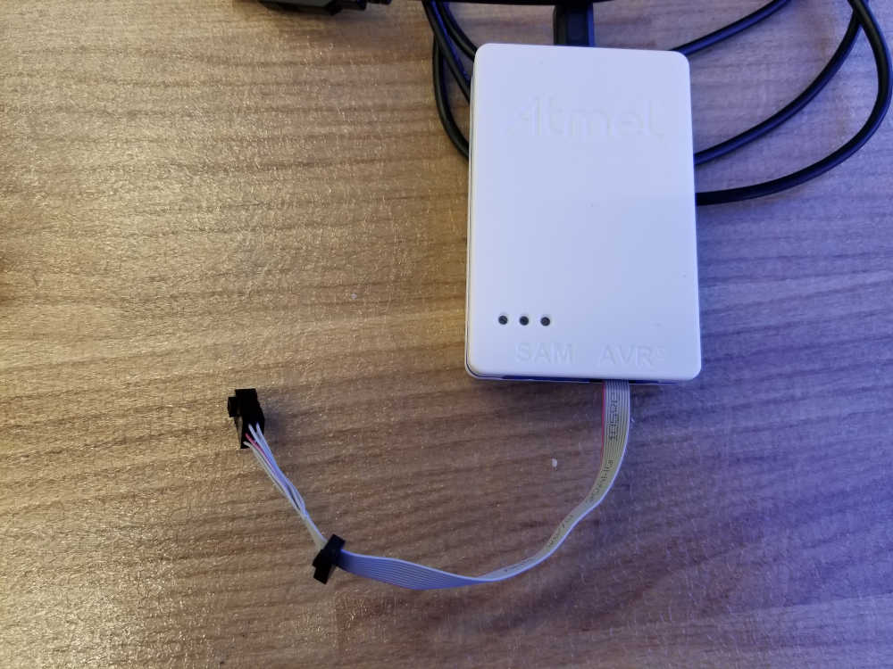
The goal of this week was to build an in-circuit programmer by milling our own PCB. Brian from 2016 has an excellent page on this process.
http://fab.cba.mit.edu/classes/863.16/doc/projects/ftsmin/index.html

PCB Milling
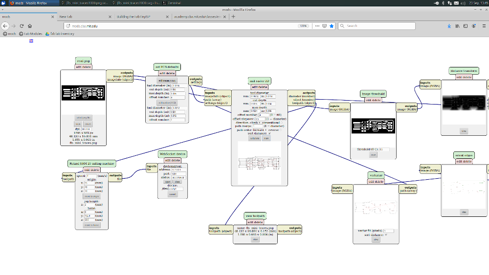
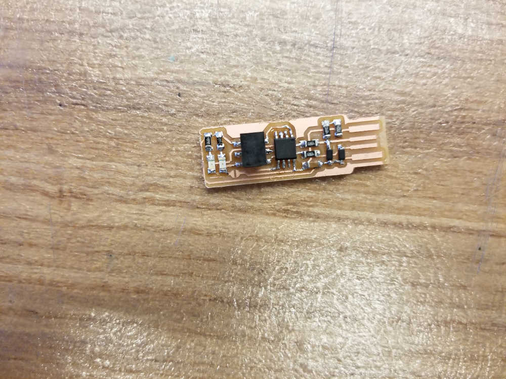
The PCB was milled using the Roland SRM20 in the EDS lab with the mods tool. The drill bit needs to be pushed into the material with a good deal of force to ensure the bit cuts deep enough. The bit will break eventually, but it's stronger than you think. The bit also needs to be held down until the collet is completely tightened. If the bit is left too high or the bit is dull, it will not cut cleanly, and burrs will be left along those traces. Those burrs can be worked off by just rubbing at them with your finger.
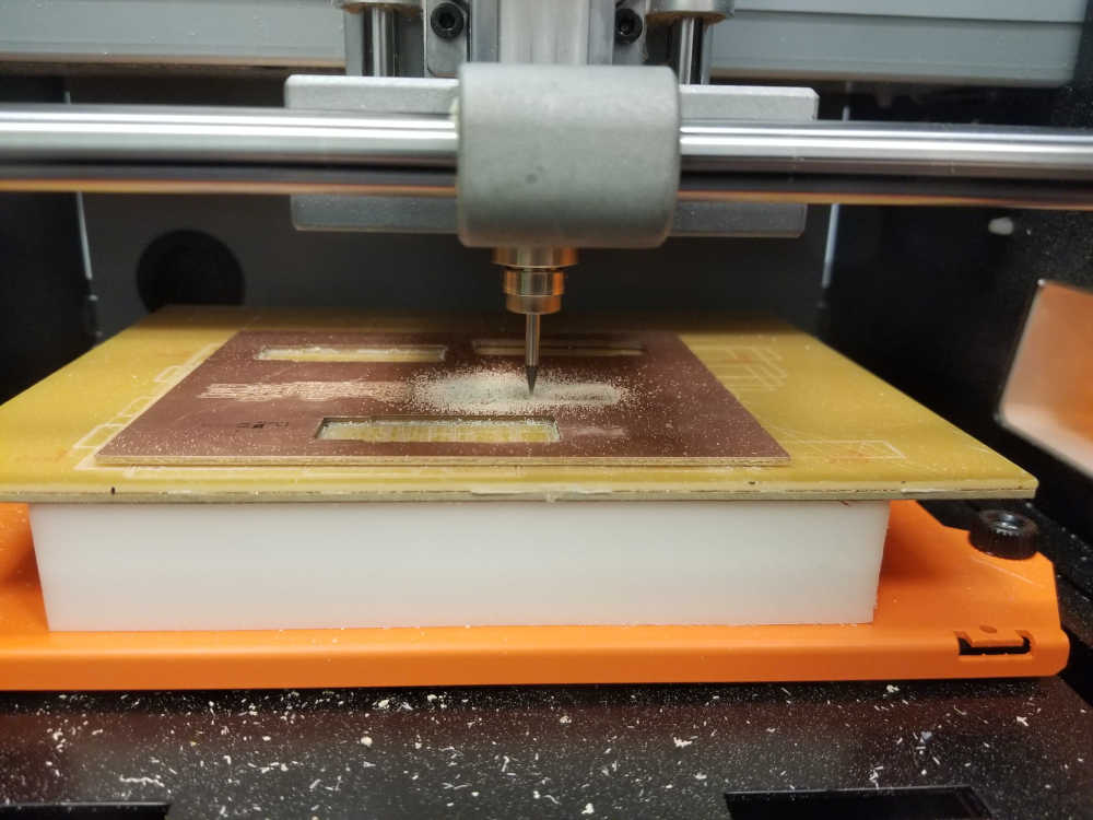
To save on time spent switching bits, I cut the traces for multiple boards at once. Keep track of your origins for each piece of you do this. Note that on this machine, the +x axis goes right, the +y axis goes back, and the +z axis goes up. The origin denotes the front left corner of the image being cut. Note that on the top right piece, I got my origin wrong by 1mm in x, so the right trace is very thin. I later soldered in an extra wire to fix this issue.

See the tutorials page for more details on electronics.
Soldering
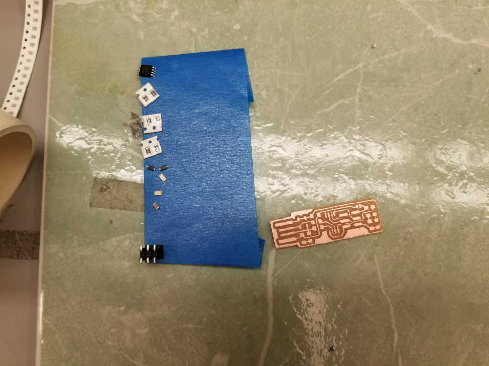
The only tips for this section are to add a bit of solder to one of the pads for each component. Then, you can solder that end down first. Go back in with tweezers and the iron to solder the part flat. Then, you can fill in the other end.
Programming
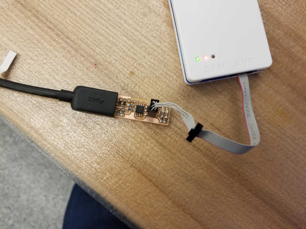
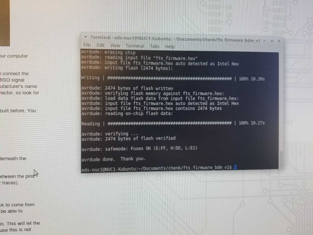
Don't forget to modify the Makefile to fit the programmer you use. Otherwise, just run the commands to program the board. At the end, you're looking for the entry which says "Multiple Vendors USBtiny". If that happens, the board is working, you can run the final command and keep going.
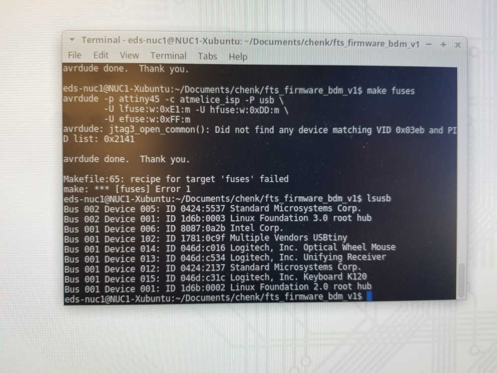
Troubleshooting
If the board doesn't show up as a usb device, you have some troubleshooting to do. First, I checked that the solder connections were even. Recall that I actually cut the outline with the wrong origin. Using a pair of snips, you can nibble down the edge of the board to match what it should have been.
If you check the image for when the board was connected, you'll see that the LED indicating power was not actually lit. That was because I soldered in the wrong resistors for the 1K resistors. Note that just because the label on the drawer is correct, you should still check the label on the parts just in case.
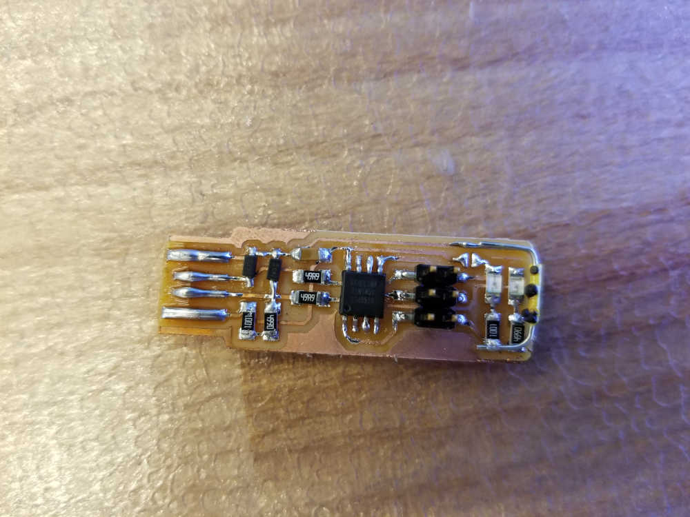
With the new resistors, the LED lights up, and the board is properly recognized.
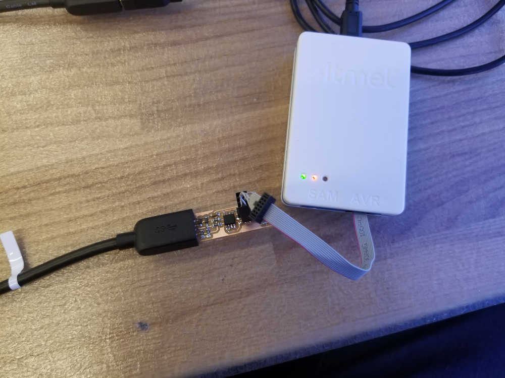
Now, that the final command has been run and the jumper has been removed, the board can act as a programmer.
PCB Milling Tests
The main limitation in this process is the bit size and the layout restrictions. These two limitations constrain the size and complexity of the possible circuits.
In the EDS lab, we can only mill boards with up to 2 layers. Even with that capability, 1 layer boards are much easier to mill. In that case, traces can only cross each other at components. 0 Ohm resistors can technically be used to allow arbitrary trace crosses, but that should be minimized. This crossing limitation constrains what circuit layouts are possible.

The other limitation is the size of the bit and the size of the traces. Typically, the milling of the traces is done with a 1/64" bit, and the milling of the outline is done with a 1/32" bit. The test traces milled on the right demonstrate some of the limitations of a 1/64" bit. The bit cuts out the dark sections. From left to right, it attempts to cut a gaps and traces with widths from 0.001" to 0.020". A 1/64" bit is 0.0156" wide. So only the gaps from 0.016" onward can be cut. On the other hand, the traces on the bottom are not constrained by the bit size. There, the limitation is the adhesion of the copper to the substrate and the cleanness of cut. In this example, the bit is a bit dull and a bit too high, so the cut is leaving a bur. However, the traces are still of reasonable quality down to 0.005" and perhaps even lower. The trace width may actually be constrained by the electric qualities of traces that thin.