week two
electronics production
characterizing pcb production
videos: characterizing milling for pcbs
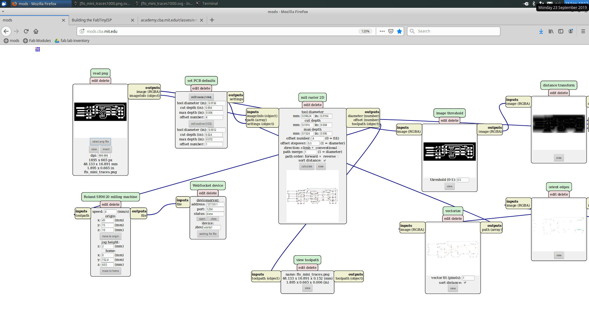
Using the mods software and the pngs found on this wonderful, life-saving info page, my group started learning how to use the Roland mill and testing the settings given by mods.
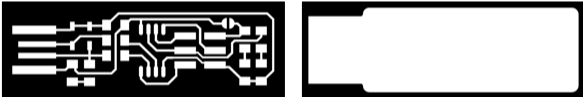
traces and outline pngs
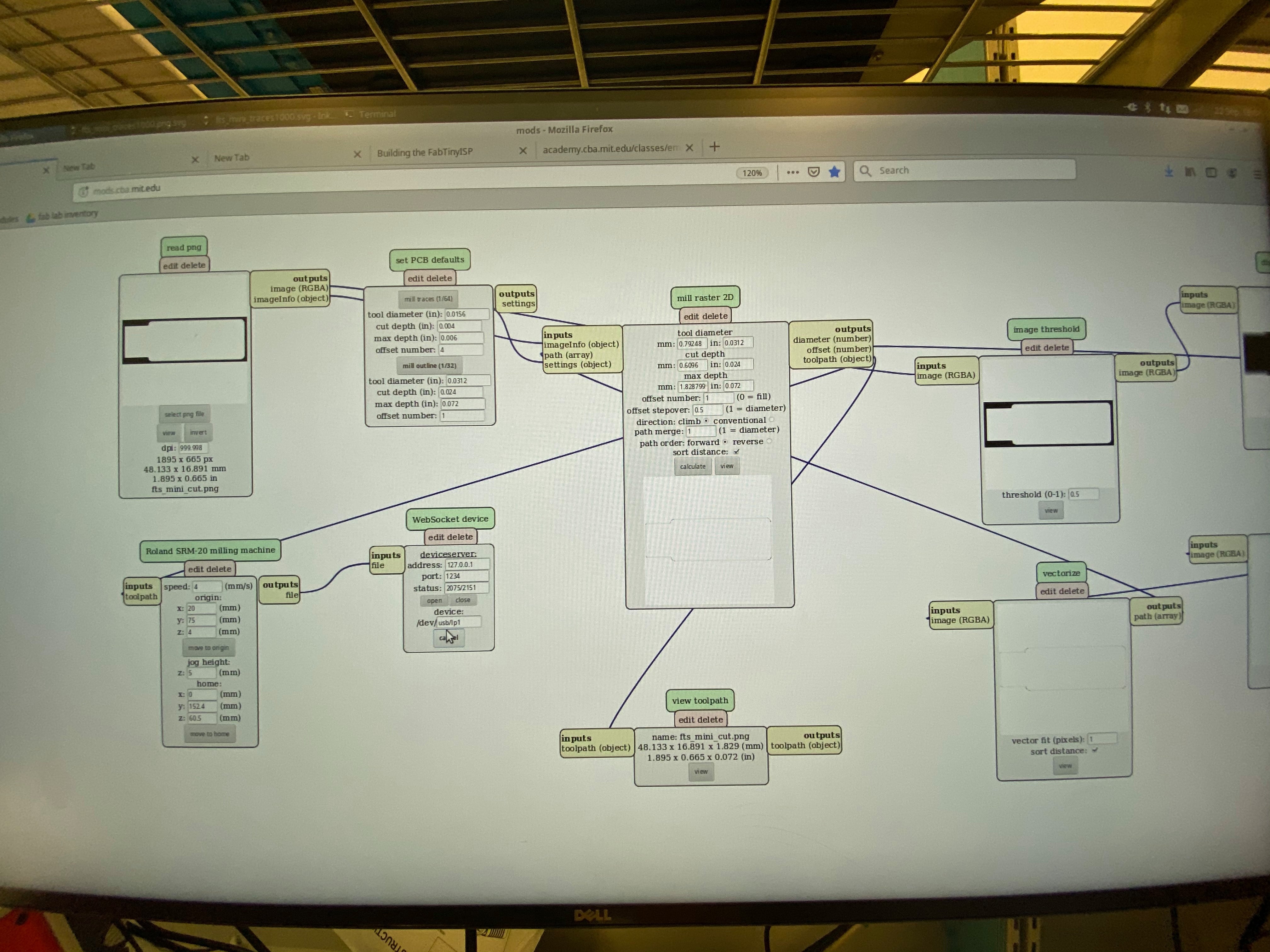
After securing the 1/64" bit and setting the origin, we used mods and its given settings to mill the traces onto the board.
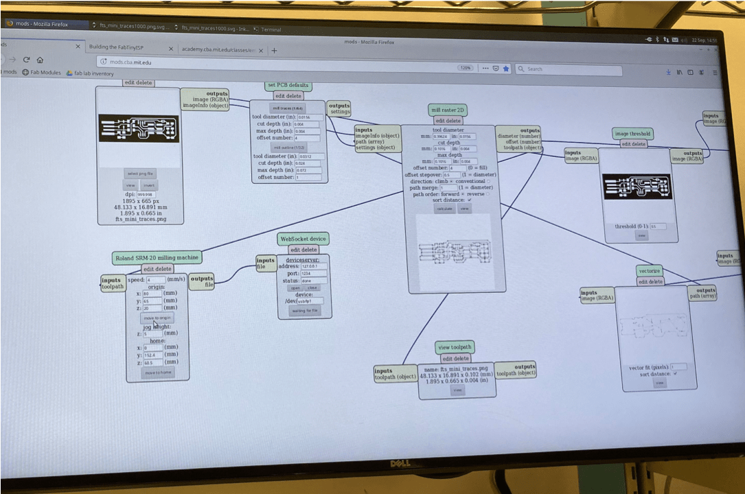
initial settings used for milling traces
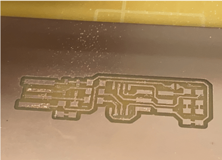
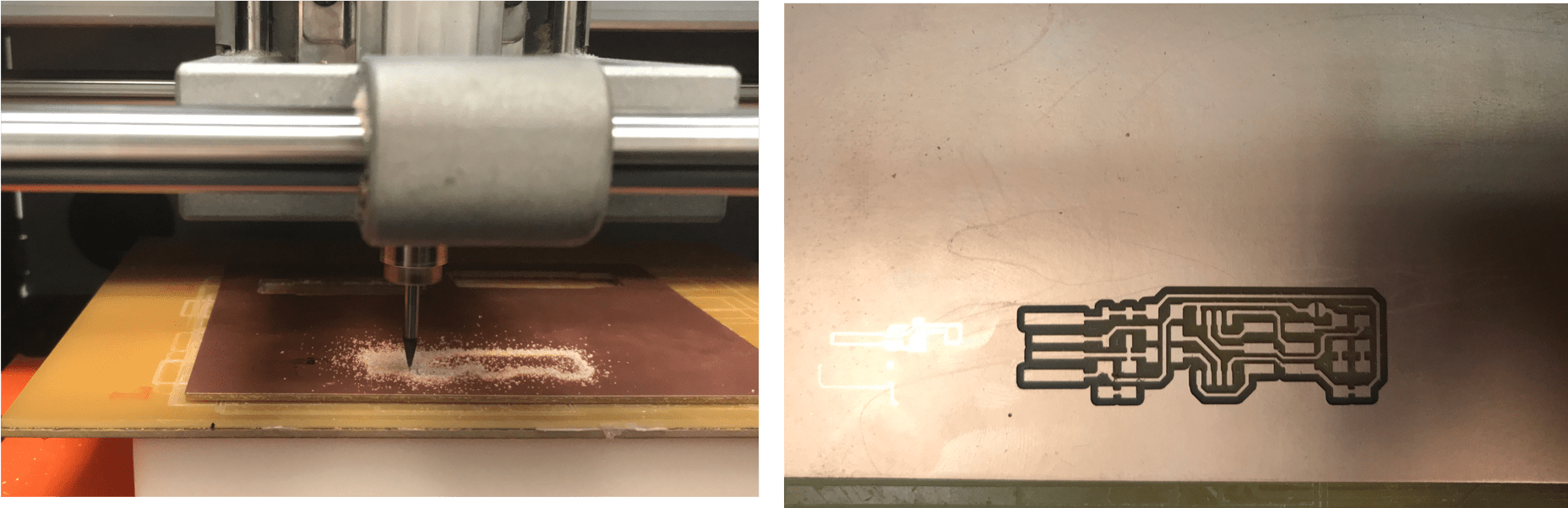
Unfortunately, this didn't turn out well. There was a lot of burring, and there was even a section that didn't cut all the way through (the shiny parts in the picture below).
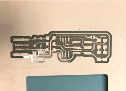
first trial
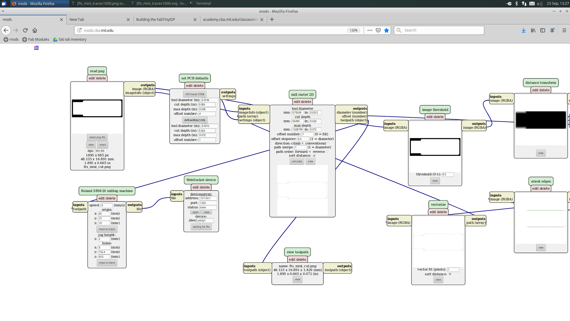
Because of this, we decided to modify some of the cutting settings and try again. We increased the max cutting depth from 0.004" to 0.006", and this actually did the trick!
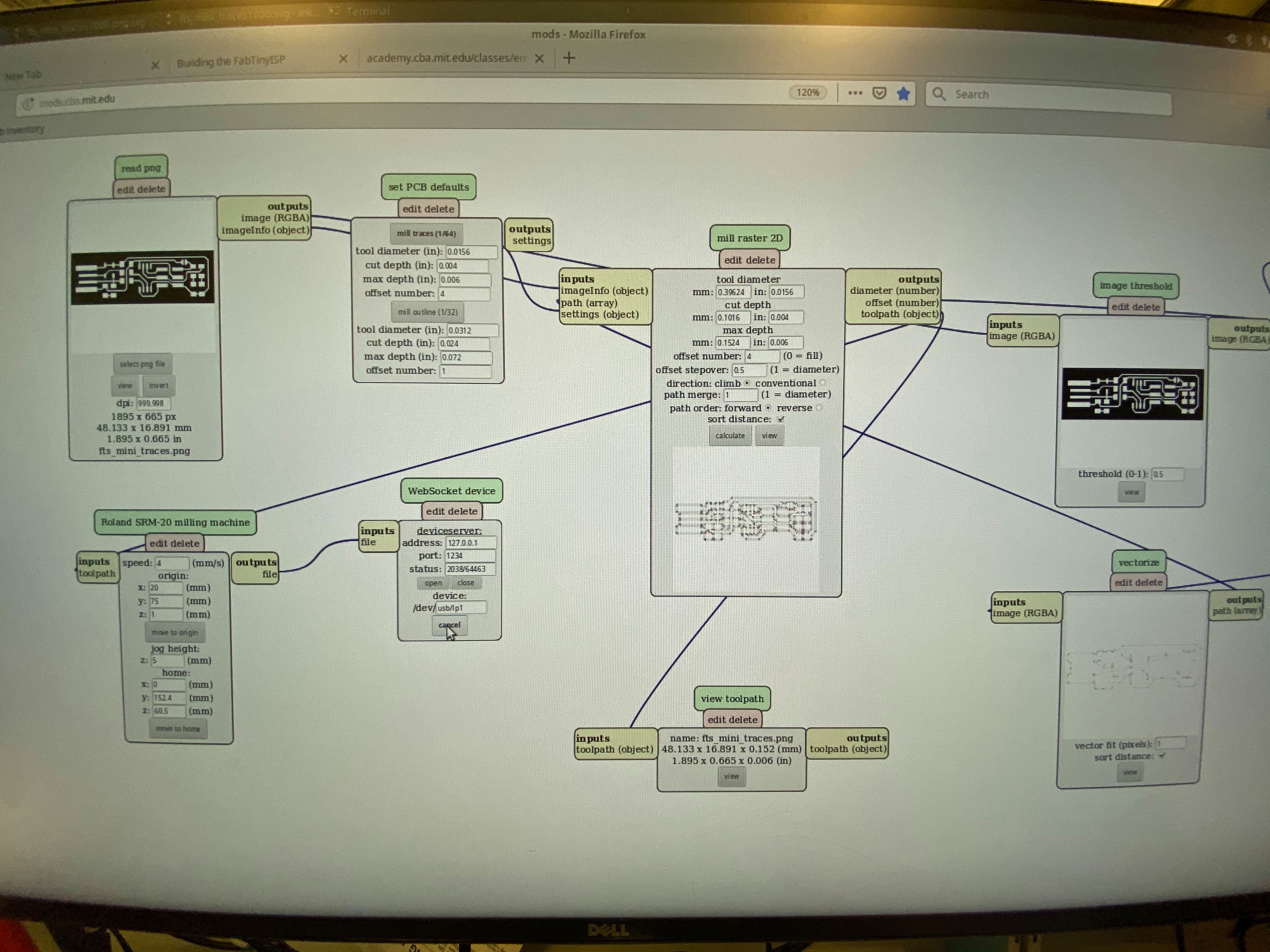
updated settings used for milling traces
second trial
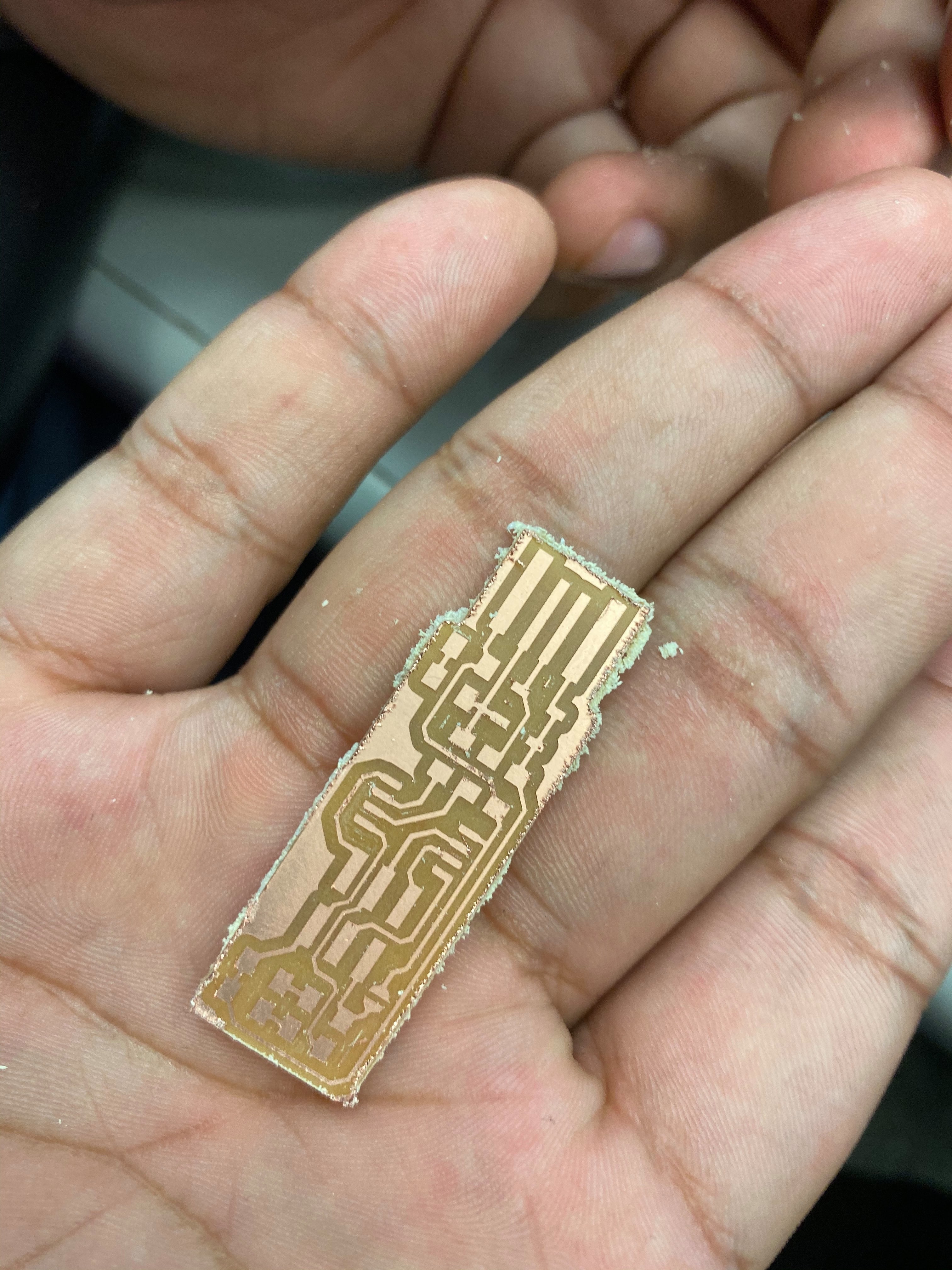
There was still some burring, but not as much as the first time, and all of the traces were cut out, so we moved on to figuring out settings for cutting the outline.
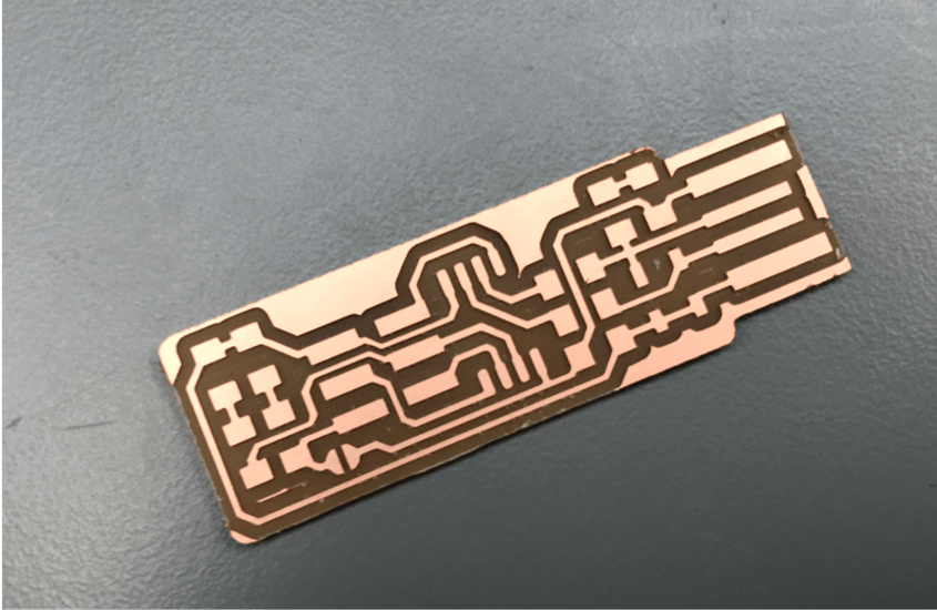
We first switched the 1/64" tracing bit out for the 1/32" outlining bit. Using the initial settings for milling outlines (given by mods), we cut out the pcb. There was some burring on the edges could've been sanded off.
initial settings used for milling outline
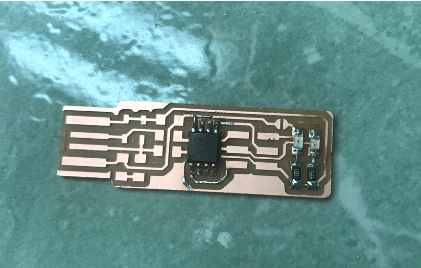
milled pcb
making an in-circuit programmer
milling the pcb
videos: pcb milling process
The first time I tried to mill the traces, I used the same settings that my group had determined the day before. However, the bit didn't cut through the copper layer, and instead etched on the copper.
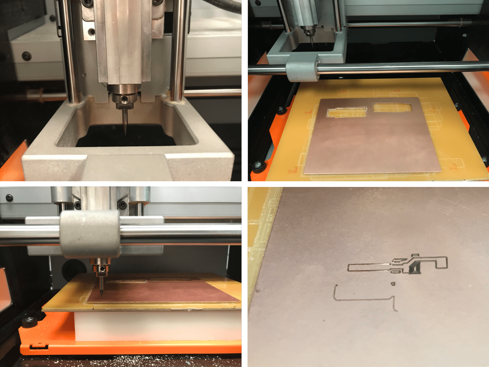
failed attempt
This happened because when lowering the bit to touch the copper, I didn't push the bit into the material enough. Instead, the bit and the copper just touched, so instead of cutting into the layer, the bit only brushed the very top of the copper.
To remedy this, I changed the origin, and made a concious effort to push the bit firmly onto the copper surface so they would make better contact during the milling process. This worked well, as the traces came out cleanly this time.
NOTE: this might've actually been the reason why the given mods settings didn't work for cutting traces when we were doing the group project. definitely did not think to press the bit firmly on to the copper surface then.
mill settings for traces using mods
successfully milled traces
Now that the traces were cut, it was time to cut the outline of the board. Taking out the 1/64" bit and replacing it with the 1/32" bit, I adjusted mods and cut the pcb outline.
mill settings for outline using mods
pcb post-milling
Before I could begin soldering, I first needed to make a few small adjustments to the board. There was a small strip of copper that remained at the tip of the board that needed to be removed. Using an exacto knife, I scraped this piece off.
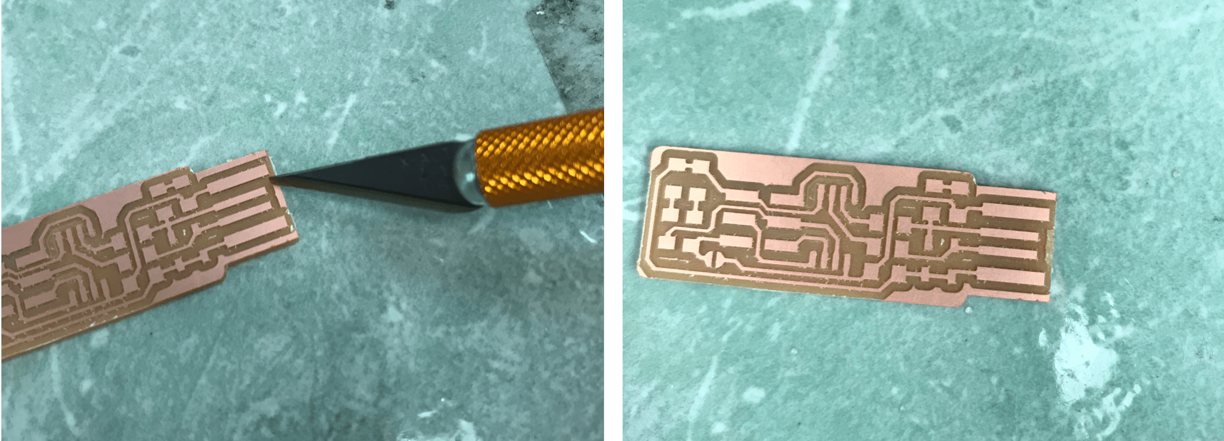
removing a small strip of copper from the board
Components used for this in-circuit programmer:
1x ATtiny45
2x 1kOhm resistors
2x 499Ohm resistors
2x 49Ohm resistors
2x 3.3V zener diodes
1x red LED
1x green LED
1x 100nF (0.1uF) capacitor
1x 2x3 pin header
Using the following schematics from (again) this wonderful, life-saving info page, I was now ready to solder components onto the pcb.
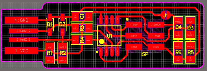
pcb diagram
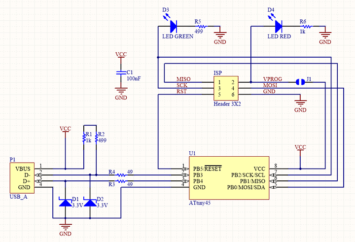
circuit schematic
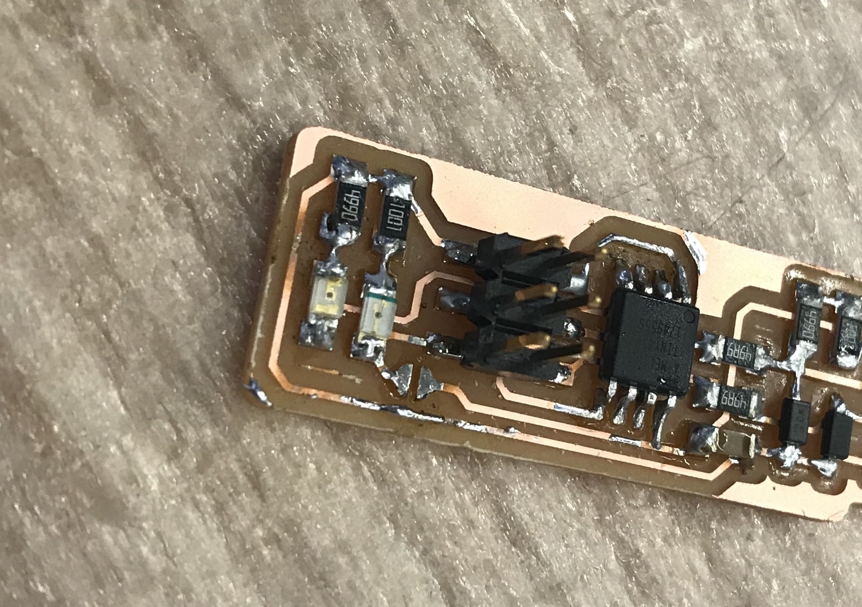
The first component I tried soldering onto the board was the ATtiny45. There was a lot of trial and error with this one, as soldering turned out to be more difficult than I expected. The components were tiny, and I don't have the most steady hands, either. However, I learned to use copper braid and the desoldering tool to clean up messy soldering jobs and eventually got the hang of it.
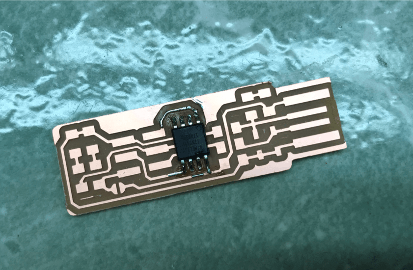
soldering the ATtiny45 on
The whole soldering got much better after someone (Alexandre) told me that the solder flows to where it can. Somehow something about this made the whole action of soldering more intuitive to me. So, instead of just bringing the solder to the tip of the soldering iron, I actually first heated up the area around the place I wanted soldered, and then brought the solder to that area and let it flow and catch onto the metal parts of the components.
NOTE: I feel like this is something you're always told to do in most soldering tutorials, so I've always known that I needed to solder like this. For some reason, it just never clicked for me before now so I never soldered correctly...huh.
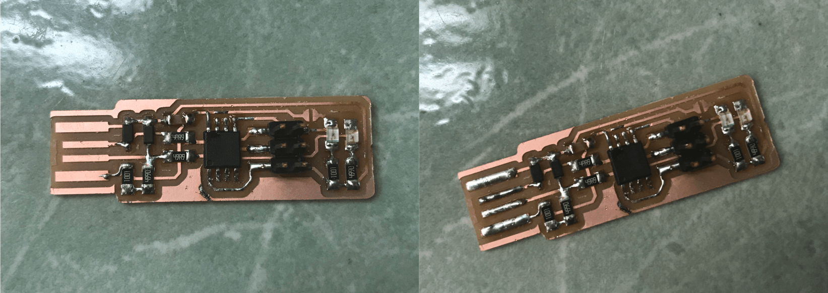
I wanted to first get all of the super tiny resistors, capacitors, and diodes on the board, and worked my way from the innermost components to the outermost.
components slowly but surely being soldered on
The pcb is slightly too thing to work well in ports, so to improve the usb connector, I flowed solder onto the usb contacts to build them up a little.
flowed solder onto usb connections to give them thickness
I had completely skipped over the part about making the solder bridge initially, so I went back and did that. The solder bridge serves as a temporary circuit short.
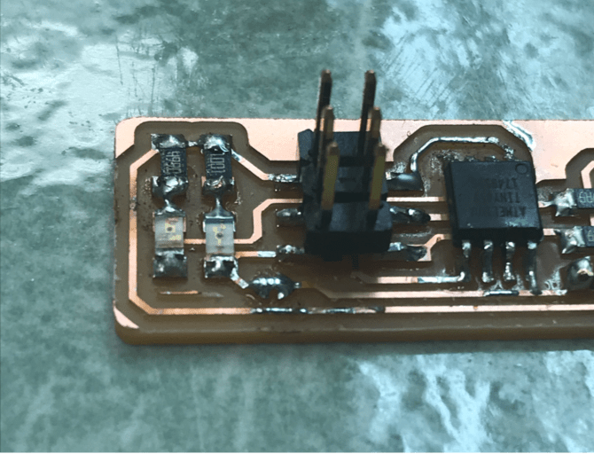
solder bridge made
With the header pins added, I was finally done soldering! Except, not really...
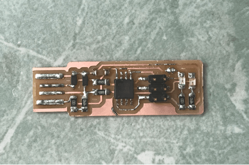
soldering is complete
Throughout the entire soldering process, I checked my work between soldering each component with a multimeter. This allowed me to ensure that I was making the connections between components that I was supposed to be making and not making those that were not supposed to be made. This cautious way of soldering probably saved me a lot of headache in the long run, too.
At the very end, when everything was soldered, I did one final test with the multimeter and found that a couple connections were not as strong. I went back and reinforced these connections, and then I was actually done.
videos: multimeter testing
programming the pcb
The programmer I used was a fabricated board that had once been programmed with the atmelice_isp (white box with blue stripe).
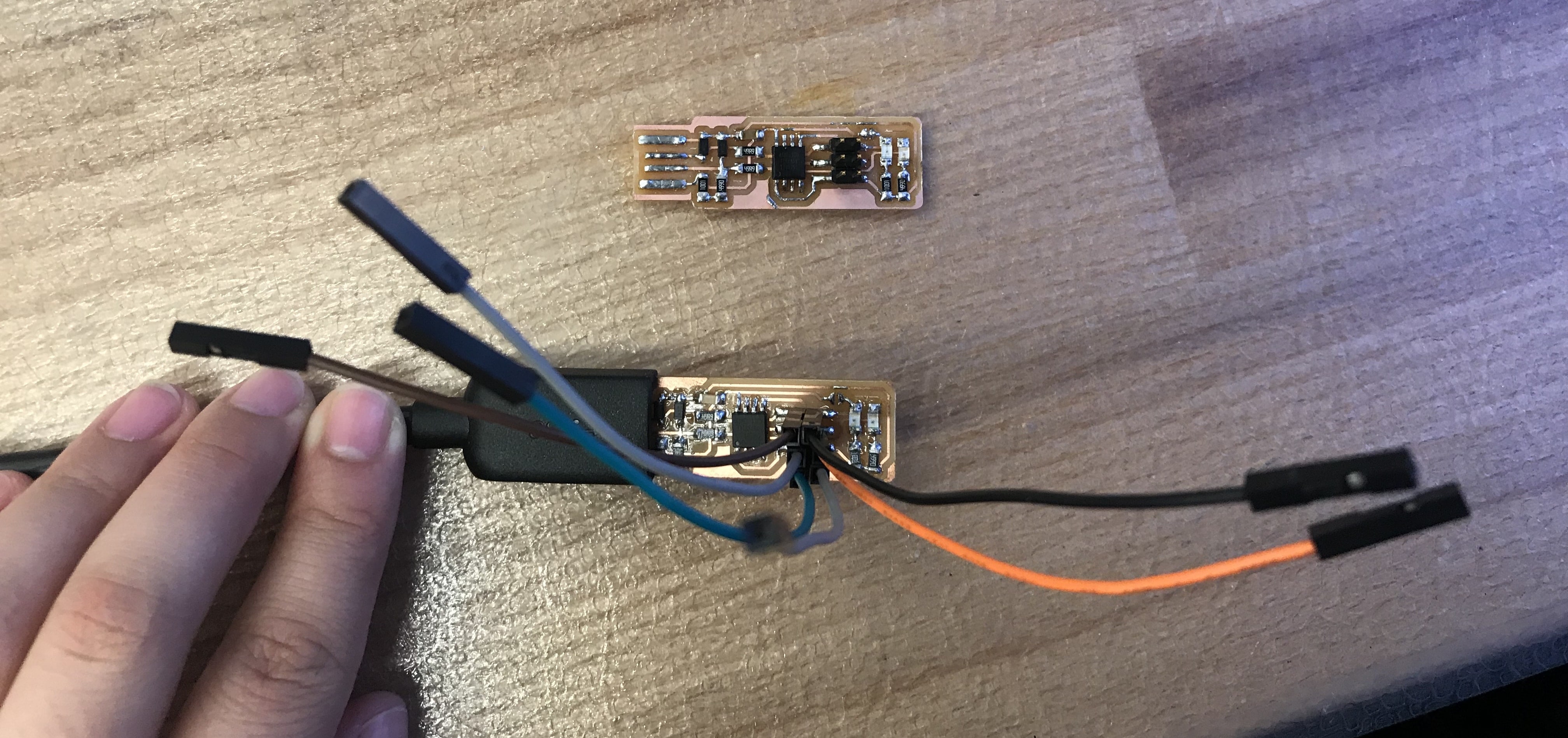
board with f-f headers is the programmer used (thanks Anthony)
Things got off to a good start, because the red LED lit up when I connected my board to the computer via USB.
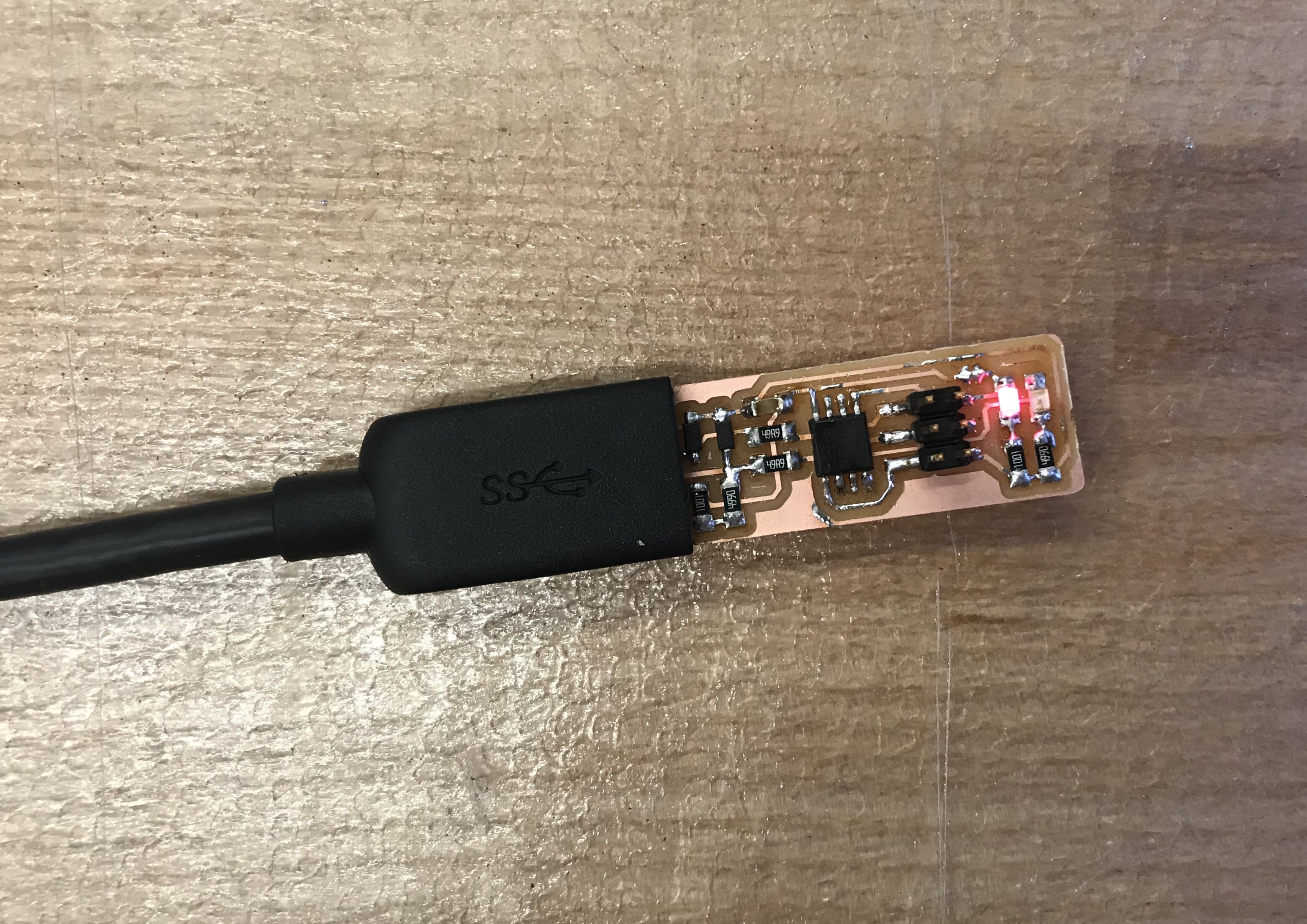
my board connected and lit up
I plugged in the programmer board into the computer via usb. Then, using female to female connectors, I connected the header pins my board with the corresponding header pins on the programmer board.
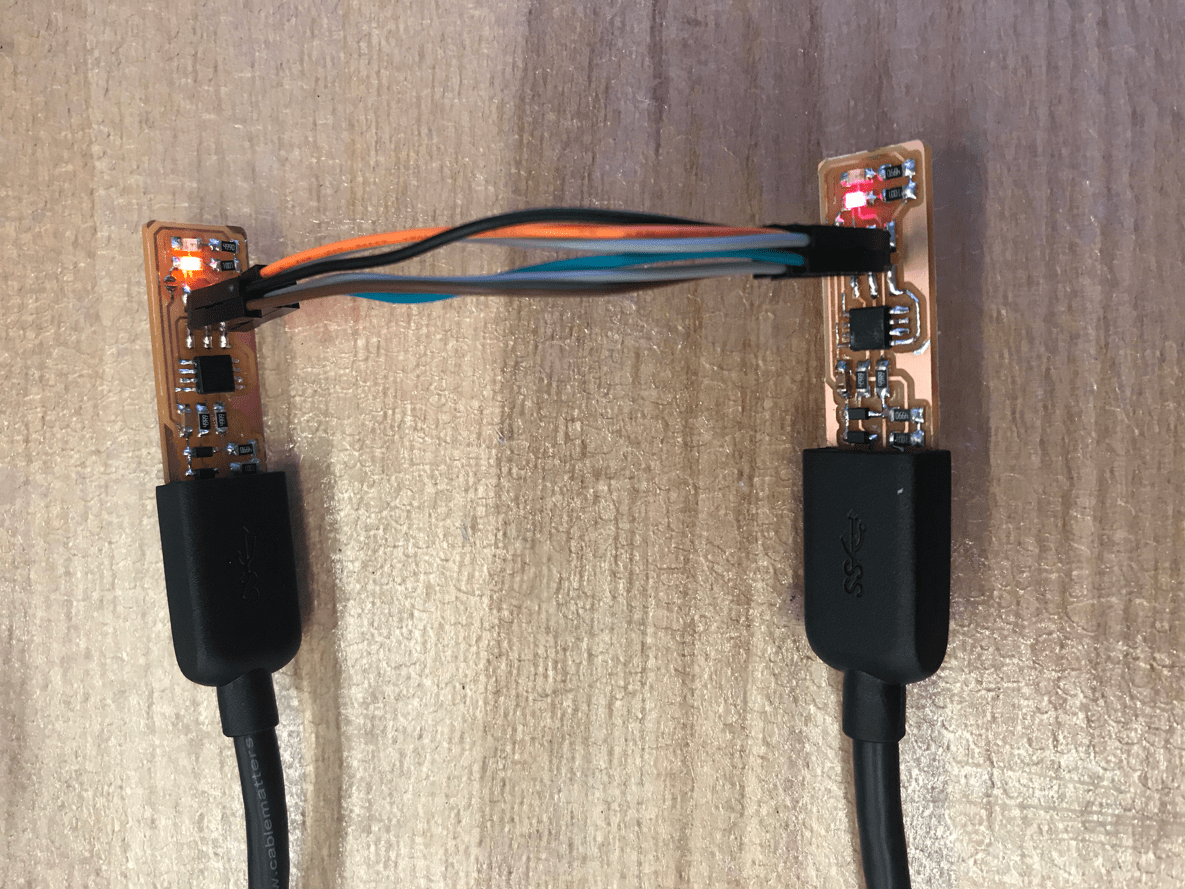
programmer and programee connected
Using Linux on the EDS computer, I downloaded the firmware source code (fts_firmware_bdm_v1.zip). The first task was to decide which programmer I was using. In this case, I was using a fabbed board with an ATtiny on it and used usbtiny.
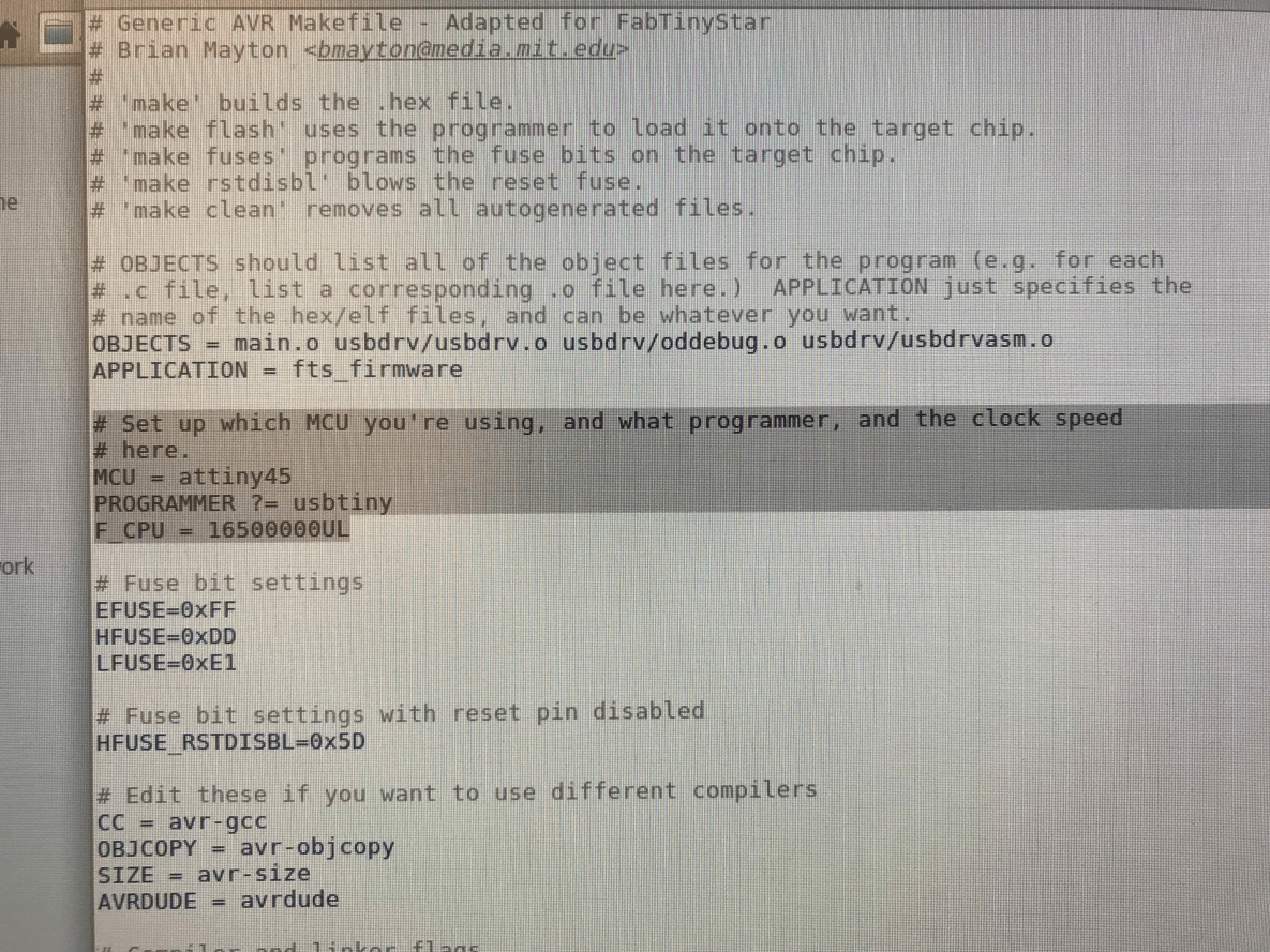
programming my board with usbtiny
I ran make flash, which erased my chip and programmed its flash memory with the contents of the .hex file built before.
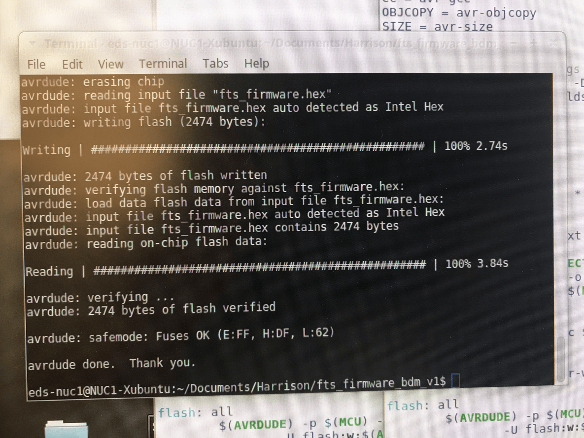
after running make flash
Then, I ran make fuses, which sets up all fuses (that control where the microcontrolelr gets its clock source from) save the one that disables the reset pin.
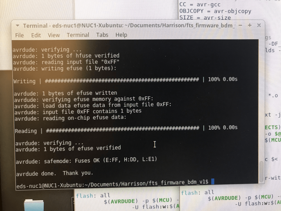
after running make fuses
After this, I needed to check to make sure that the USB on my board worked before blowing the fuse that would enable my board as a programmer. Unplugging the programmer from my board and typing lsusb in the terminal revealed my device as "Multiple Vendors USBtiny", which means it worked!
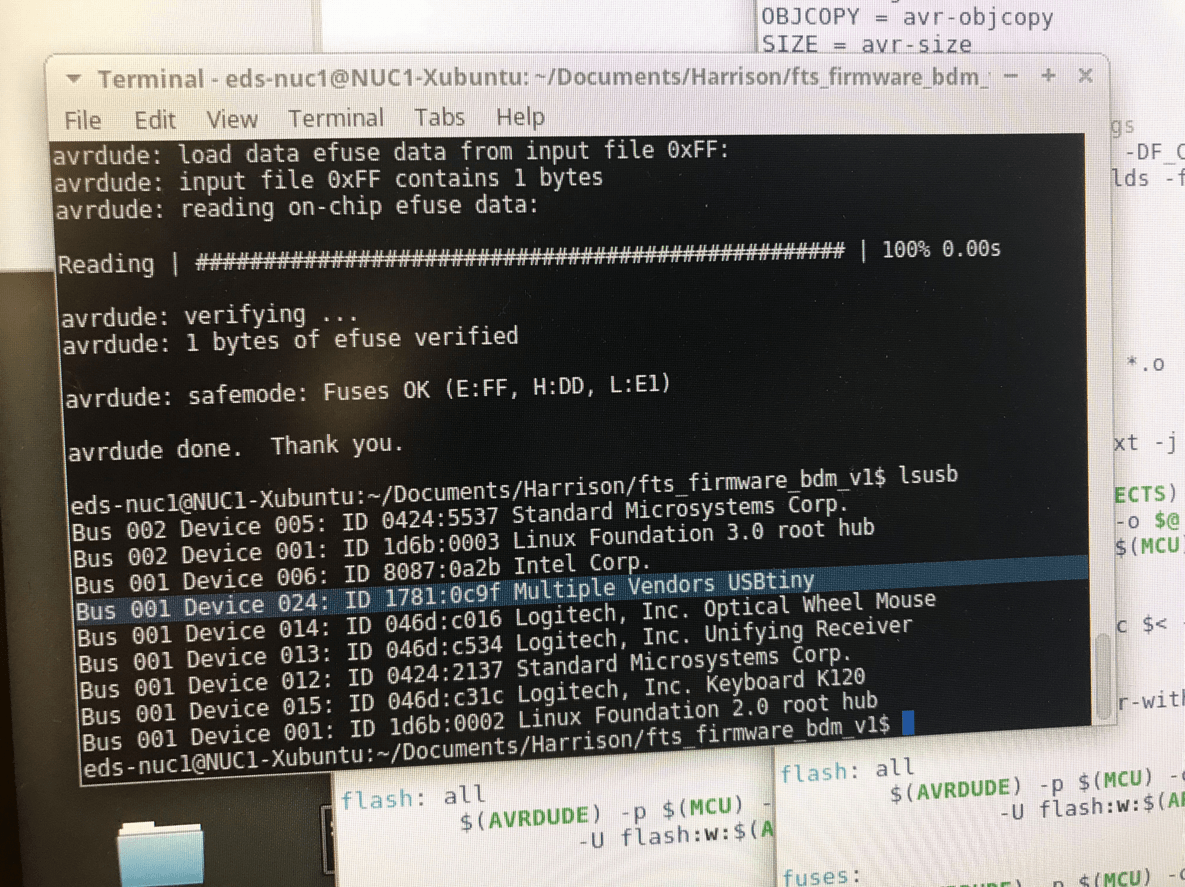
the usb on my board works
videos: programming worked
Then, I was ready to blow the reset fuse to turn the programee into a programmer. I ran make rstdisbl, which turns the ATtiny45's reset pin into a GPIO pin. This disables the ability to reprogram the ATtiny45 on my board in the future.
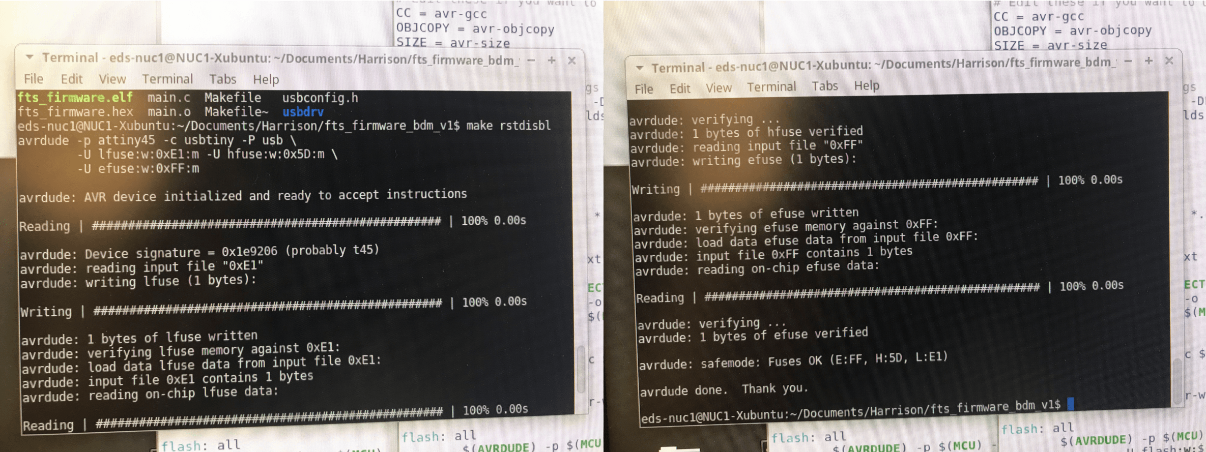
after running make rstdisbl
The final step is to remove the solder bridge on the board, which disconnects Vcc from the Vprog pin on the ISP header. I used a desoldering braid to do this. And yay! We now have a programmer!
solder bridge no longer