MILLING:
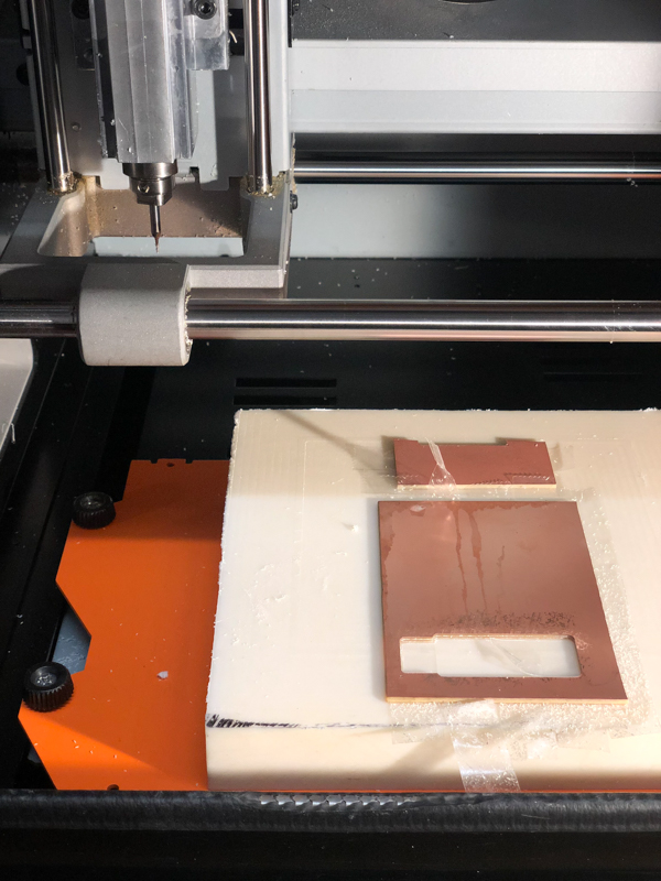
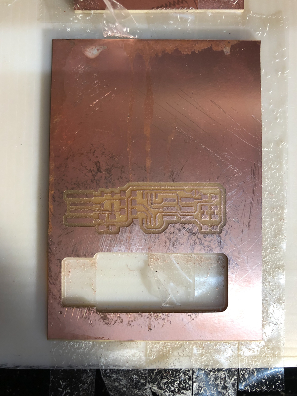
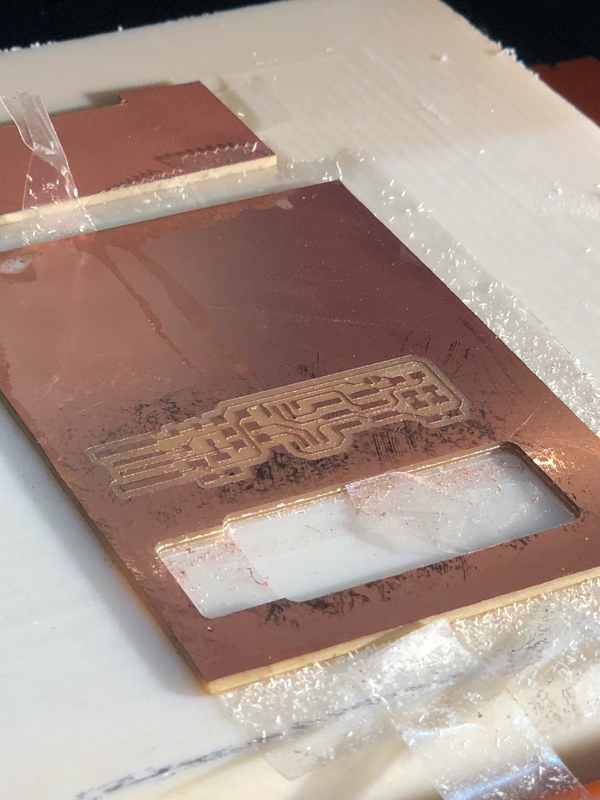
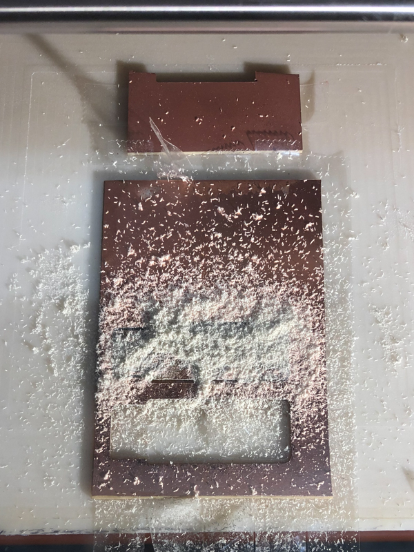

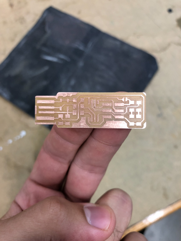
The electronics assignment this week involved the CNC milling and production of FabTinyISP’s. Using a Roland SRM-20 desktop mill and MOD software from HTMAA, a copper composite board was fixed to the mill table and machined with two end-mills and operations. The initial cutting, intended to remove the topmost copper layer, was machined with a finer carbide end-mill, whereas the cutting pass was accomplished with a more robust carbide end-mill. My board required one additional pass to remove the copper layer, as the initial cut depth of .004mm was not sufficient. I changed that depth to .0045mm, which sufficiently removed the remaining copper.
SOLDERING AND PROGRAMMING:
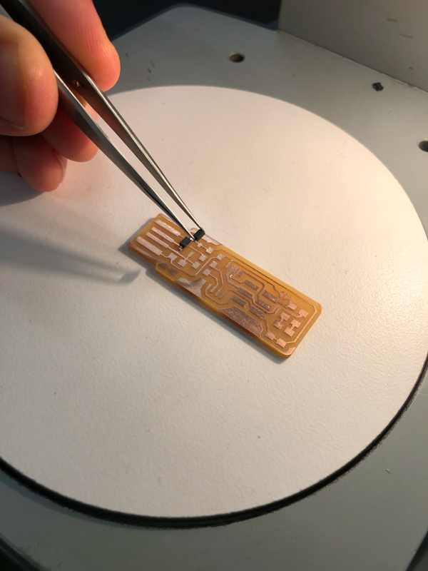

After milling, I referenced Brian’s instructions and proceeded to solder the assemble the printed circuit board. The USB connector was improved by adding solder. Additionally, a sublayer of vinyl was added beneath in order to improve the contact and friction when the USB was in use.
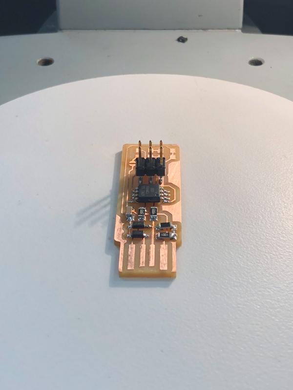
FINAL PRODUCT:
