This week, we transitioned from referencing an existing PCB design to using one that depends on schematics and designs of our own. We were given the task of re-designing or re-drawing the echo hello-world board, with some simple additions such as LED's and a button.
I began using the example board layout provided, which shows what components are necessary and a potential base layout.
I used Eagle software by Autodesk for this assignment, given Rob's recommendation and given that the student license is free (for now).
The FAB parts library was downloaded, which helped streamline things hugely. It seems as though Eagle and software like it are powerful tools for optimizing the production of complex circuit boards. Very cool.
Moving parts around in eagle was quite difficult, as was maneuvering the wiring in to other components. All in all, however, it was helpful once I became more familiar.
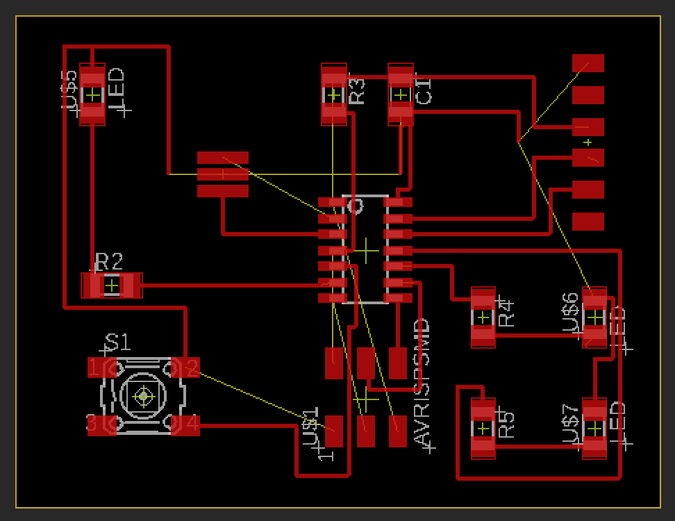
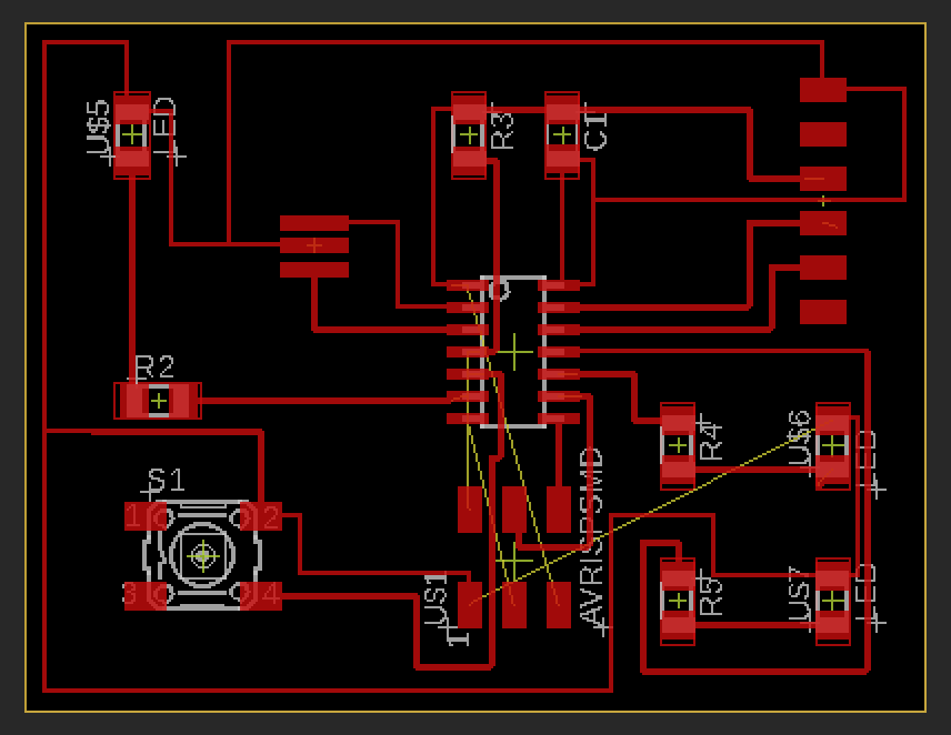
Three LEDs were added to the design rather than one, along with associated resistors.
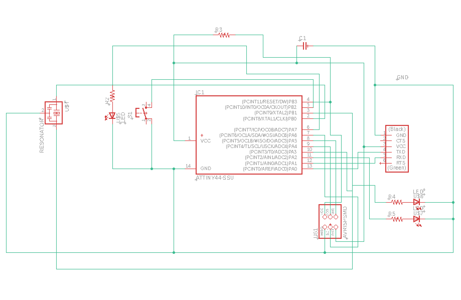
Developing the schematic was interesting, in that I initially expected that schematic to be translated visually to the eventual design of the circuit board. Upon finding out that this was not really the case, it made an interesting connection between architectural drawing and sketch models or architectural models. There are connections between the two, but representation often takes differing forms depending upon the medium.
Per recommendation from Rob, I referred to Julia Ebert's page from 2017. It is a hugely helpful resource.
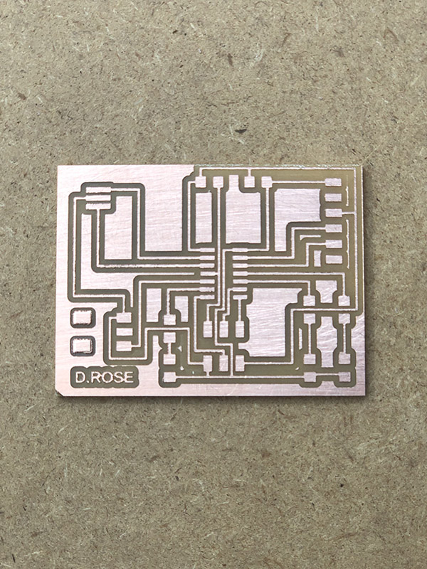
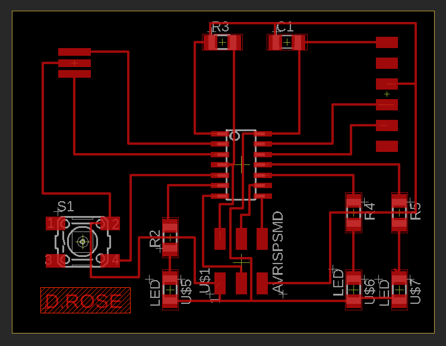
Schematic:
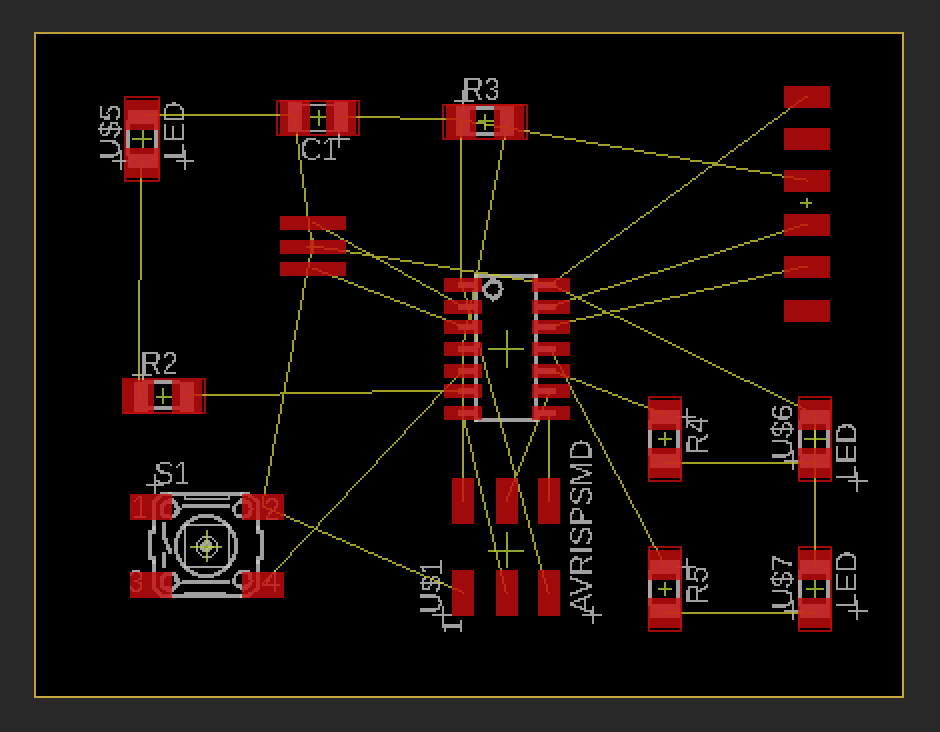
Iterations:
I also chose to record and attempt a few different iterations of the circuit board based on differentiated linework techniques and also sorting through what works and what didn't. One ambition is to develop a massive circuit board for the sake of beauty and visual interest. In short, how do you make a beautiful circuit board at the scale of a work of art?
After many attempts, I managed to create a wiring design that not cause issues or require cutting into the copper on the underside of the board.
Once complete, all layers were turned off aside from the Top layer. This was exported to a PNG with 1000 dpi.
After this, the outline layer was also exported to a PNG. Note, in order to export, it seems as though you may actually need to draw an outline. Pro tip.
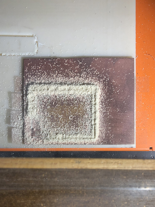
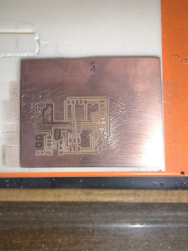
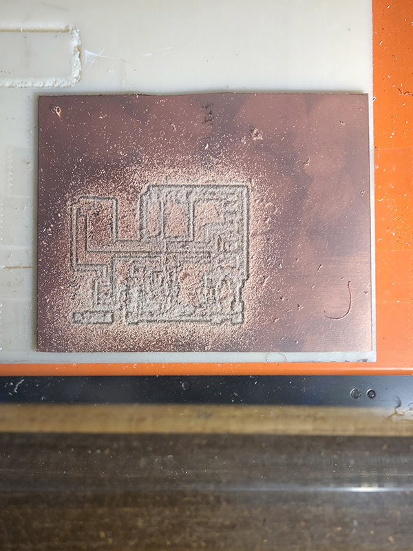
Milling and Soldering
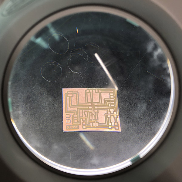
Milling of the PCB board was fairly straightforward, as the fabrication process form week three remained largely the same. I used the Roland SRM-20 mill with a 1/64 inch endmill for machining the finer details and removing the topmost layer of copper from the composite substrate. While trying to be diligent about keeping the end in place while tightening, I manage to still have an unusually high cut level, requiring a second pass of machining. Keeping in mind that this occured previously, I lowered the Z cut depth to .045mm, however, needed to do a second pass at .052 mm in order to fully cut through all of the copper material. Rob suggested that the endmill may have been spent, which could have caused some issues as it relates to machining quality. Some of my board for instance retained a black color around areas where the endmill travelled, potentially implying burning of the layer beneath.
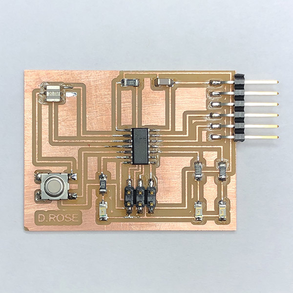
The soldering process was again very soothing. I chose to design this PCB in a larger format manner, which also made it quite easy to solder. The result (I think) is quite clean.
With two other classmates, we also programmed the new PCB and reviewed Julia's terrific descriptions.