Week 4: Electronics Design
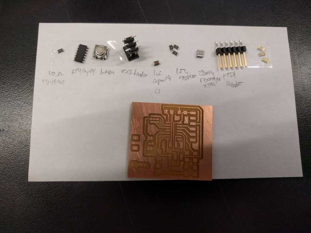
This week's assignment is to redraw and make the echo hello-world board and add a button and LED (with current-limiting resistor).
PCB Design
Summary: This week I designed and made my own PCB.
First, I read about how electronics basically work and will need to learn more to better understand what I’m doing. In section, I downloaded the Eagle PCB design software and imported the FAB parts library (a compact inventory of necessary components). I started by adding all the hello-world components to my schematic, including the 3 LEDS each connected to a 1 kΩ current-limiting resistor, a ATTINY44, resonator (clock), button, and more. As I wasn’t sure what to do, I followed Julia Ebert’s documentation and schematic and board design. I wish I’d known how to connect each part to another by creating label names to declutter the green lines because the “rat’s nest” got complicated overlaps fast.
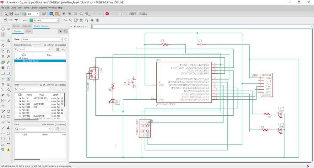
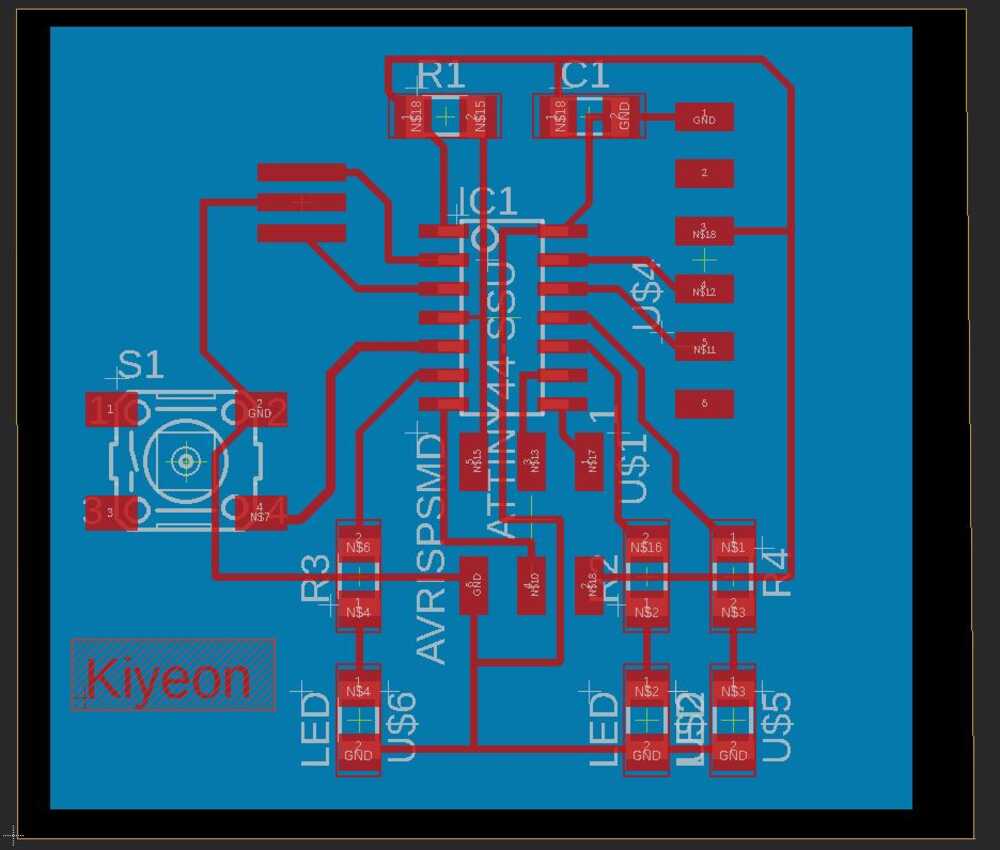
After double checking that each component was properly connected in the schematic, I moved to designing the board layout according to Julia’s board layout. Maybe I should’ve simply only added one LED. I moved the parts closer together compactly near the origin. I made the mistake of wrongly orienting the parts (so the lines did not connect). Also, I understand that the ground parts should all connect and other lines should not intersect. Also, it seems that my lines are too thin, so I’ll increase the line width from 6 to 15. Also, although I needed to squeeze in three lines inside the ATtiny44, the outer two lines were almost touching the board. To space out the lines more evenly, I changed the grid size to 5 mil (0.005”) for a finer adjustment. The lines need to be spaced out at least .015 inches, so there should be at least three boxes (each with a length of 5 mil; turn on display to see boxes). For fun, I added my name using text. I compactly reduced the black space and created a rectangular outline by changing the layer to Bottom.
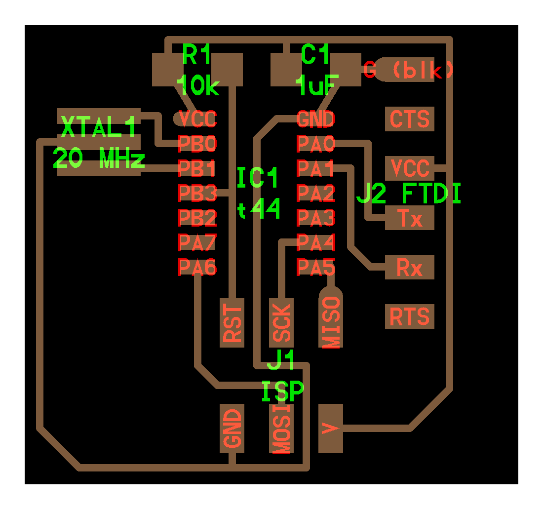
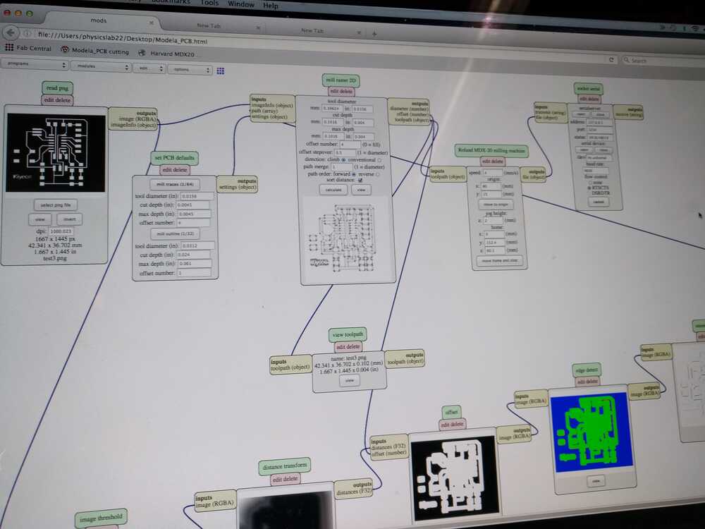
To convert the board design into PNG files to mill, I turned off the visibility of all layers except for “Top.” Then I exported the design and outline, checked the monochrome box, set the resolution to 1000 dpi, and saved.
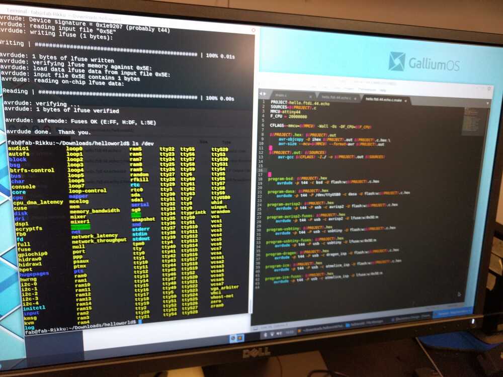
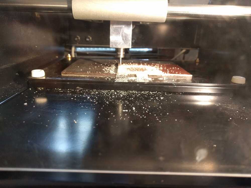
Milling: I needed a refresher on how to use the milling machine. In general, following the instructions posted to the wall was helpful. Had some difficulty with getting the machine to start. Remember to set origin. Start with the diagram (1/64 shallower) first and afterwards mill the outline (1/32 deeper). I milled according to the electronics production week procedure.
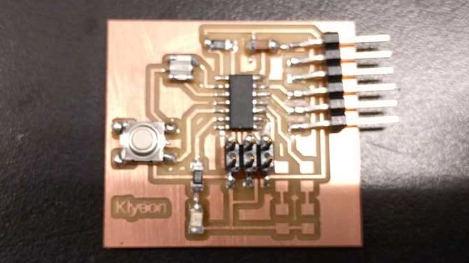
I tested this and it worked great for the embedded programming week.