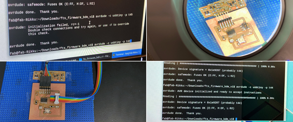
The assignment consisted in redrawing an ftdi.44 board, adding a button and a LED and testing it. I started by downloading Autodesk Eagle Version 9.5.1 and getting acquainted with the with the application. Then I uploaded the library from the fab lab containing the specs of all the components needed to design the board. Then I analyzed the different components used on the diagram of the electronic board to be redrawn and identified them in the library. Components needed (label in the library): 2 resistors (R1 10K), 1 Capacitor (C1 1uF), 1 Resonator (X Tall 20MHz), 1 Tiny 44 (IC1 t44)m 1 2x5 Connector (J2 FTDI), 1 2x3 connector ISP (J1 ASP or AVR_ISP), 1 Bouton (6mm) and 1 LED. I then created a new schematic, imported each of these components and positioned them to mirror the original board. I used InDesign to allow me to visualize the numbered inputs and outputs in each of the components and the connectivity between them. I used different colors in my InDesign diagram to makes it easier to see how I needed to draw the nets in Eagle’s schematic file. After I generated a board, a new window opened visualizing the footprint of each of the components and outlining the inputs and outputs to be connected following the drawn nets. My goal here was to position each of the components in the most optimum place thinking that nets could not overlap. I then retraced each of the nets to redesign the final board taking into consideration spacing to allow milling restrains. I was then adviced to change the width of each of my nets from 6 to 10 or 12, as the wider the nets, the less probability to break them during the milling or soldering processes. I then grouped all the elements and placed them close to the origin to avoid wasting material, made sure all these were drawn on the “top” layer, created a “bottom” layer and traced a rectangle to outline the cutting edge of the board. At this point I exported each layer individually as an image giving them 1000 DPI resolution and saving them as .PNG files.