Introduction:
This week we were tasked with designing a circuit PCB and manufacturing it.
Workflow
Plan: Begin by drawing a schematic in Eagle, arranging it on the Eagle PCB layer, and soldering everything together.
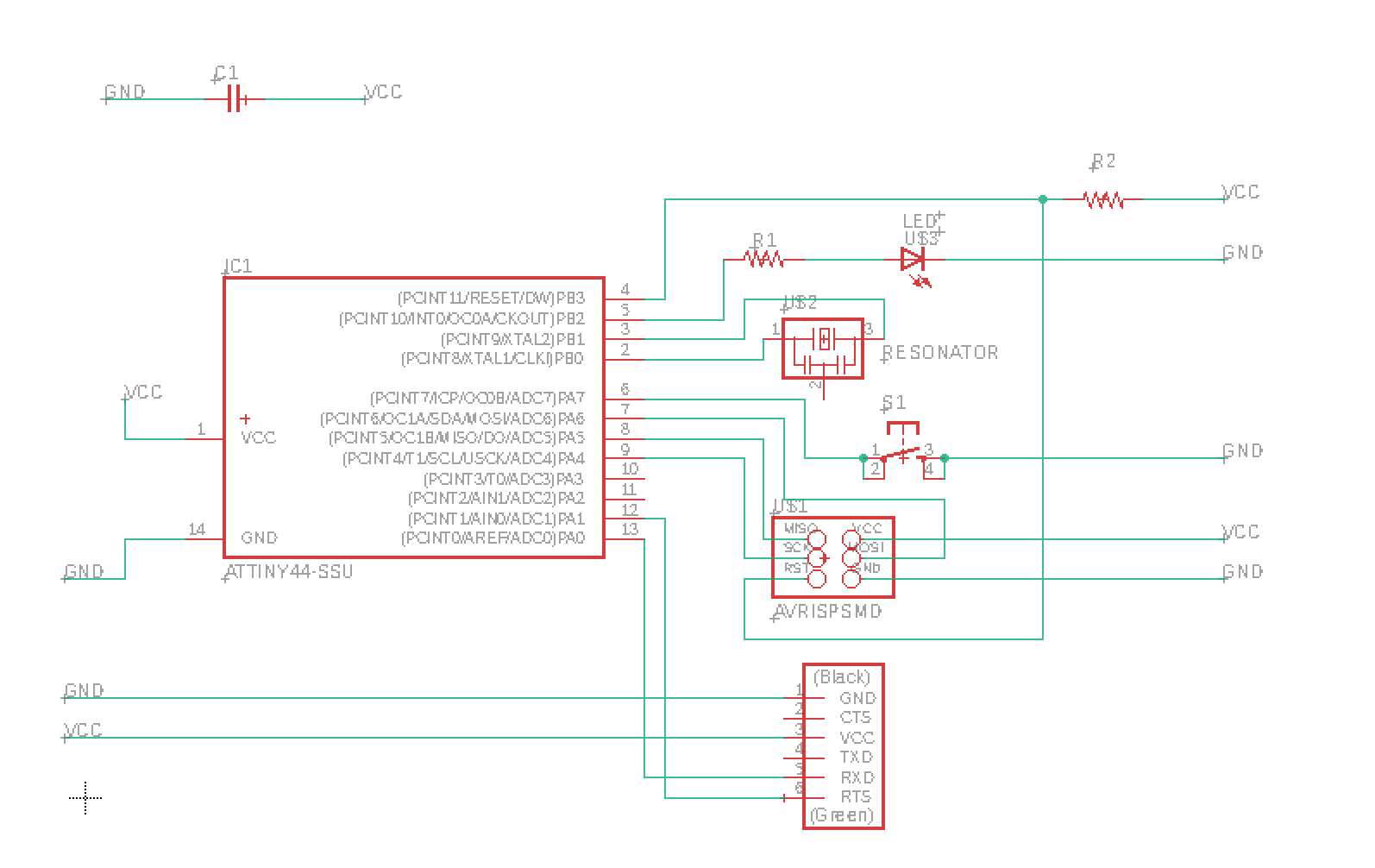
Schematic
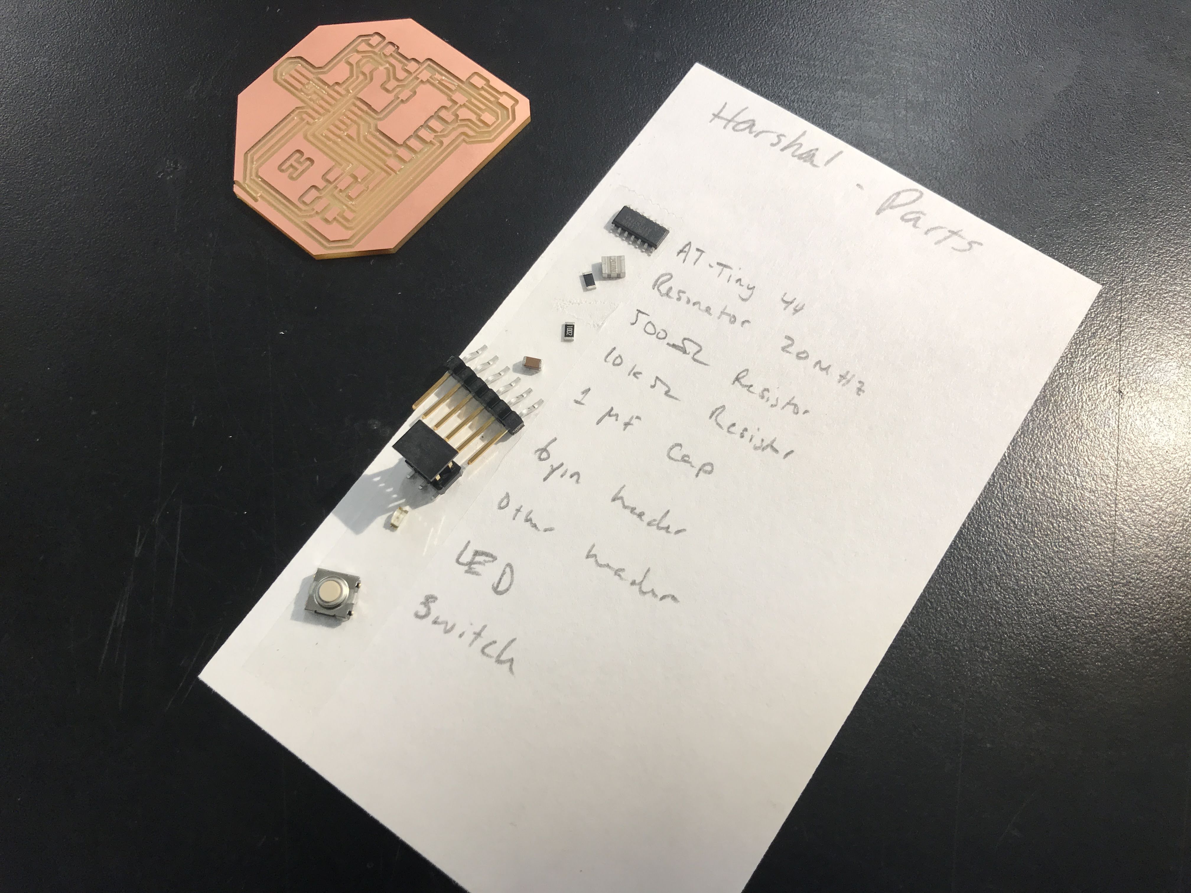
I began by importing all the parts I needed for the hello world board and placing them on my field.
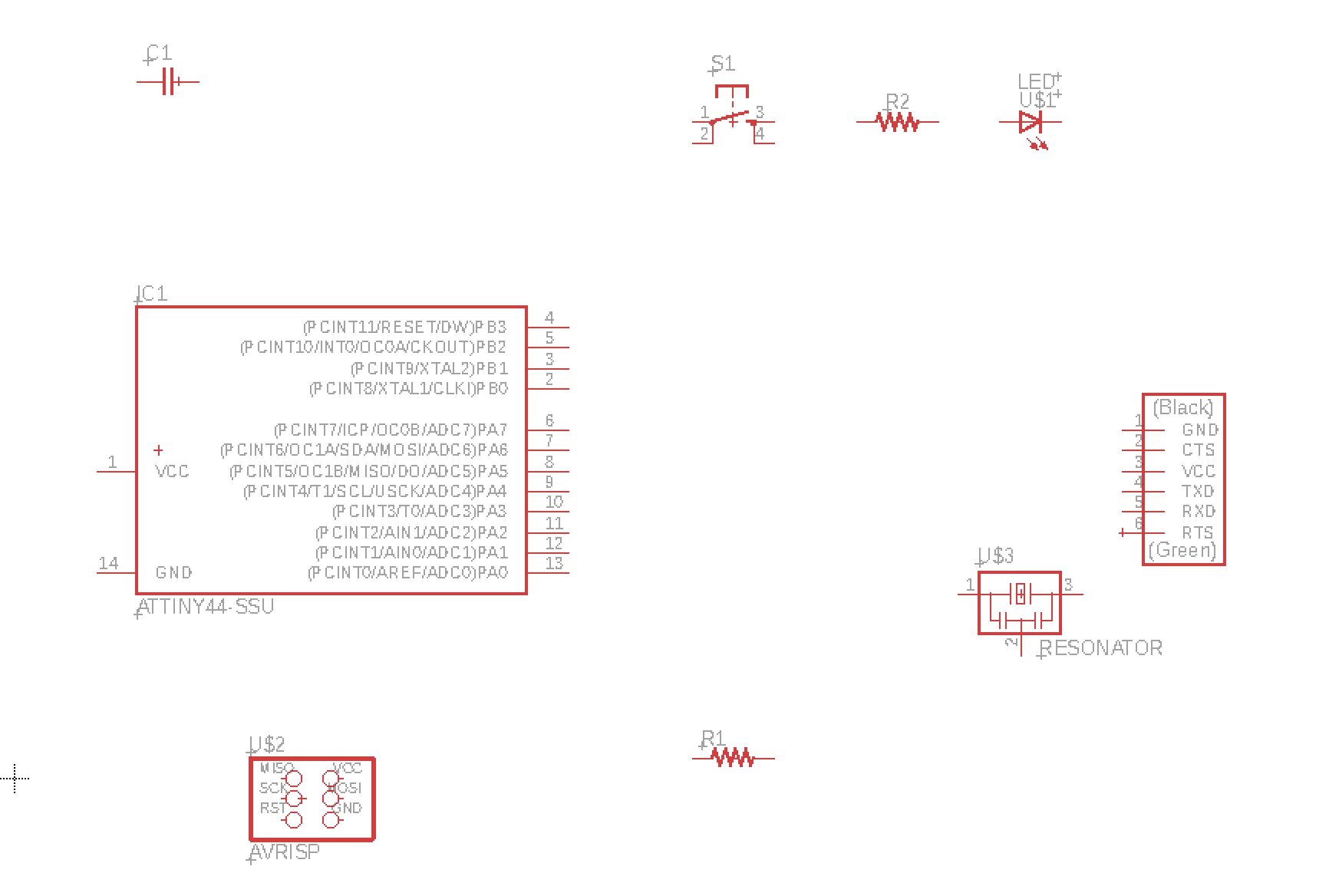
I added the remaining parts and began connecting them together. I used schematics from previous years, as well as part datasheets to help me identify where to place connections.
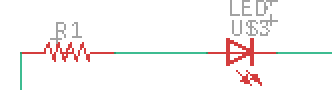
When adding my LED, I knew I needed to identify a resistor value that would get the correct voltage drop, and after looking at the LED datasheet, I settled on a 500 ohm resistor.
After my schematic was all ready, I was ready to move on to arranging it all on copper.
PCB Design
Eagle offered us a simple way to turn a schematic into a PCB, and leaves it to us on how to route the connections. RATSNEST and collision avoidance helps with this greatly.
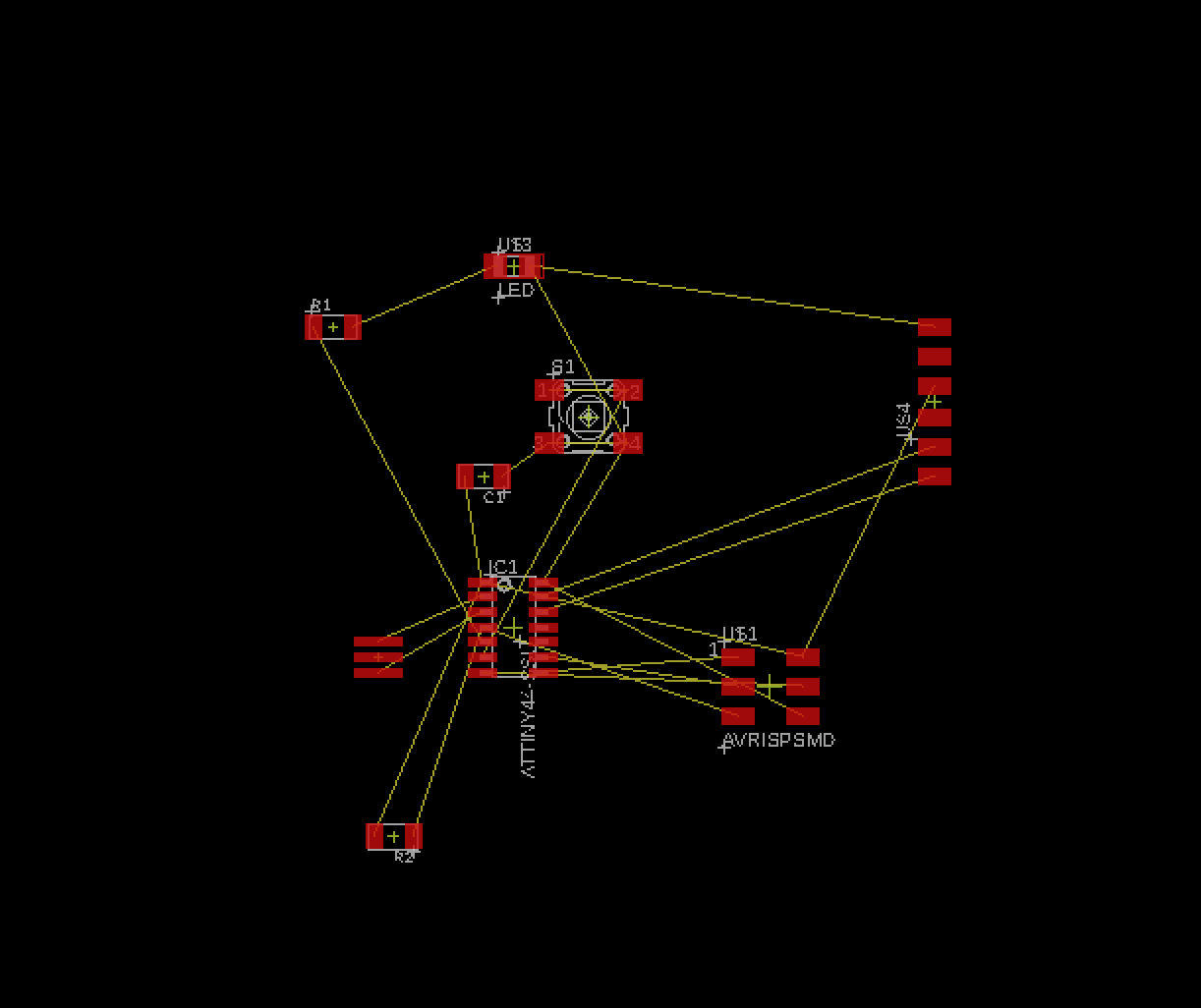
This was after routing about half the parts. My strategy was to start with the ATTINY, and route things clockwise around it.
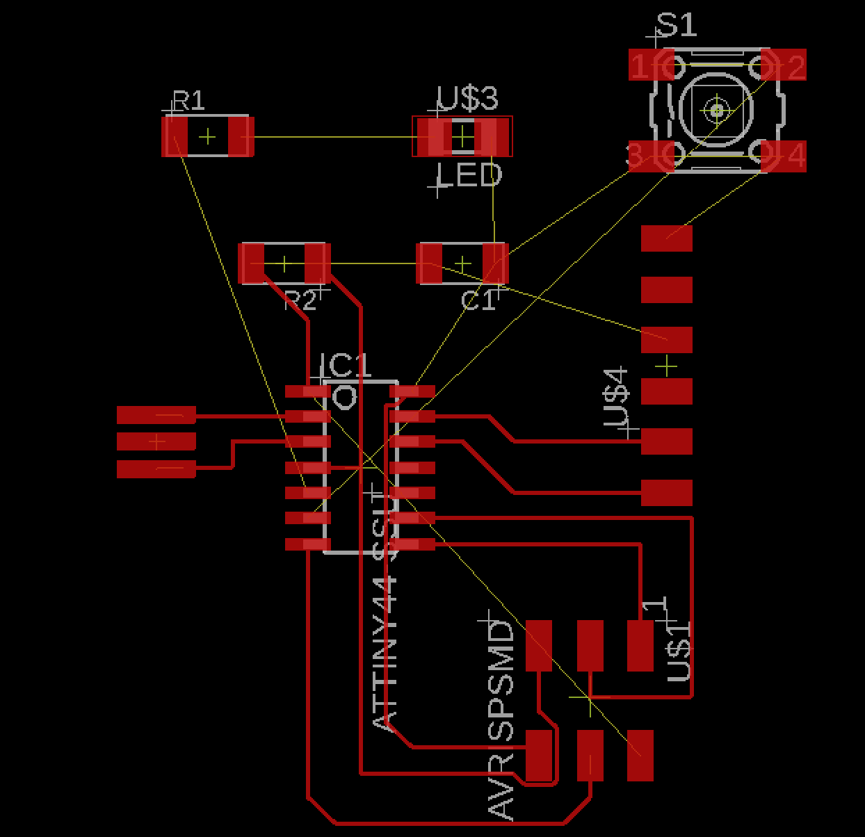
I ended up with the following nest.
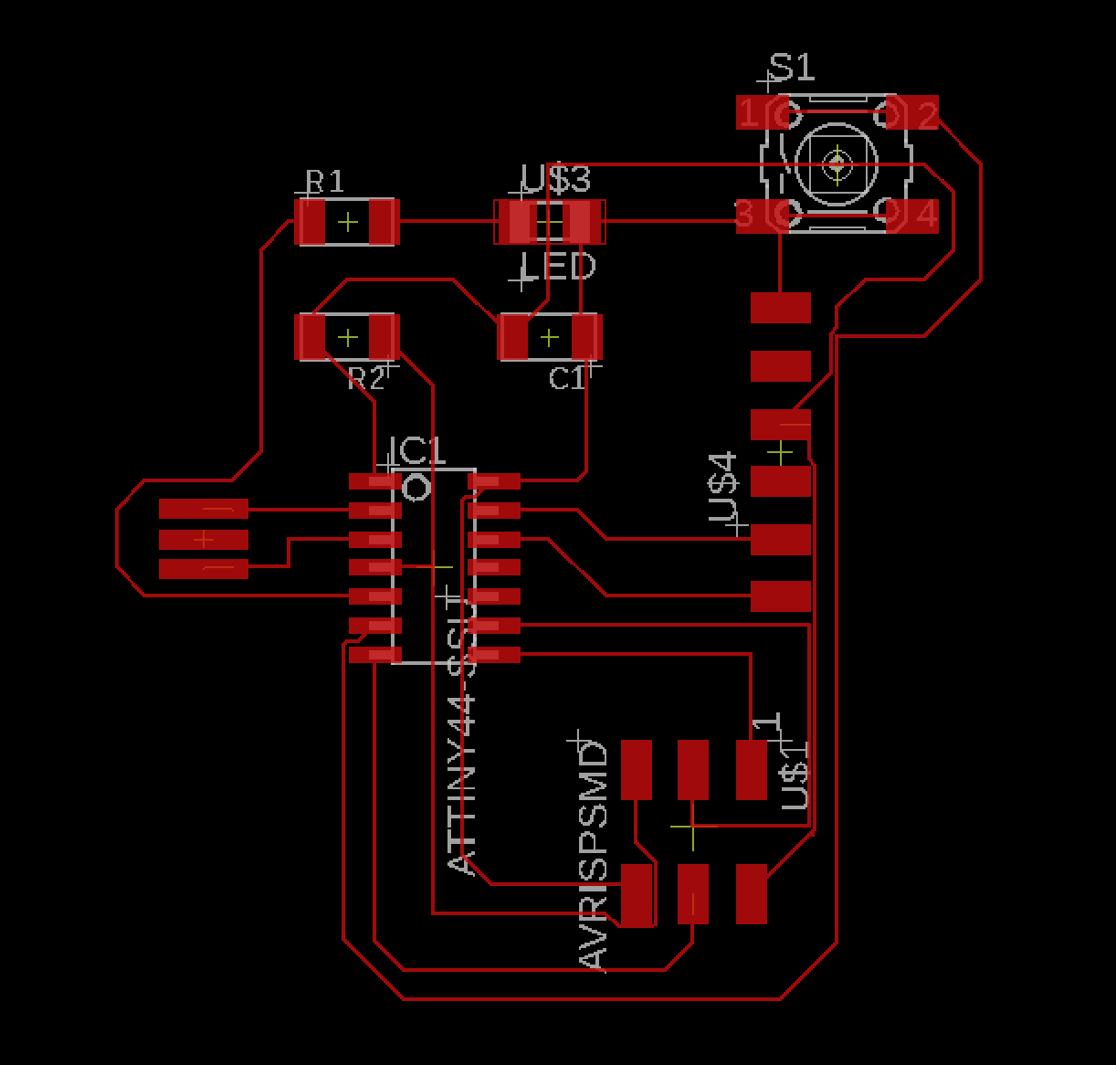
I saw that the grid Eagle locked me into put some of the routes very close together. I resized the grid to be as fine as possible, and manually moved around the last few connections. I also drew a border to cut it with in a different layer. I like the 45 degree angle cuts.

I was pleased with the final product. If I could do it again I would be more cognizant of sizes. I could've packed this all much closer.
PCB Manufacturing
This was a nightmare this week. I went through an embarrassing amount of copper (Sorry Rob!) to get this week's project to come out properly. Most of the mistakes were on me.
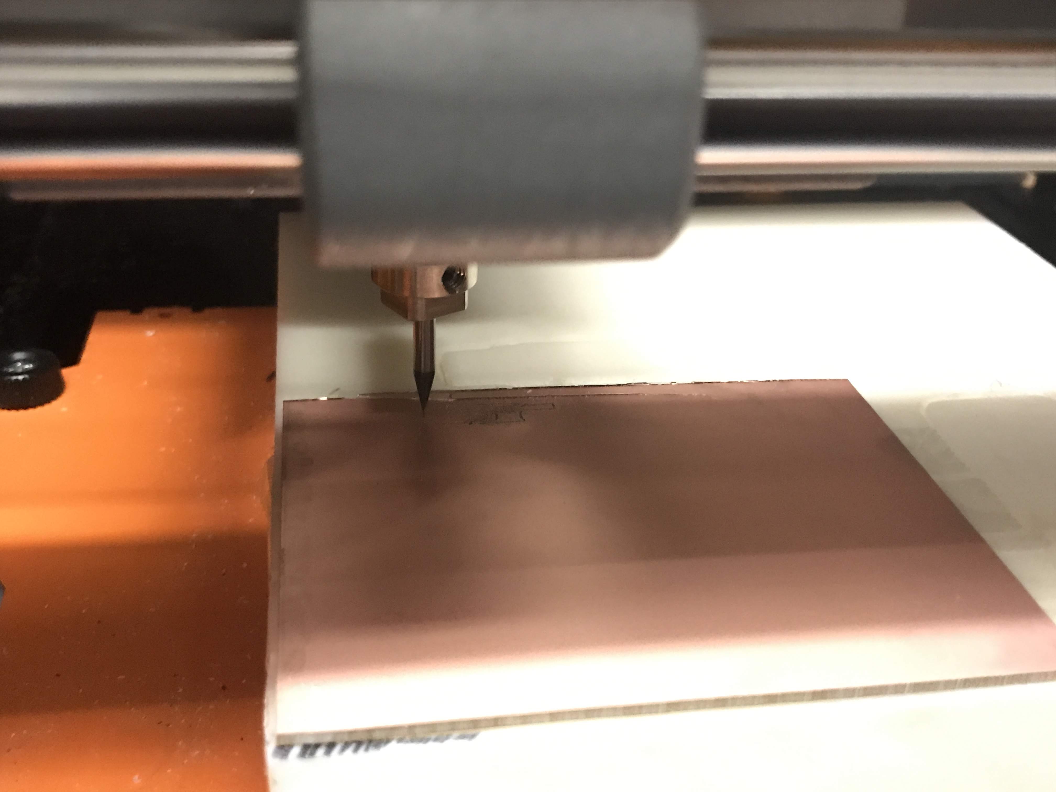
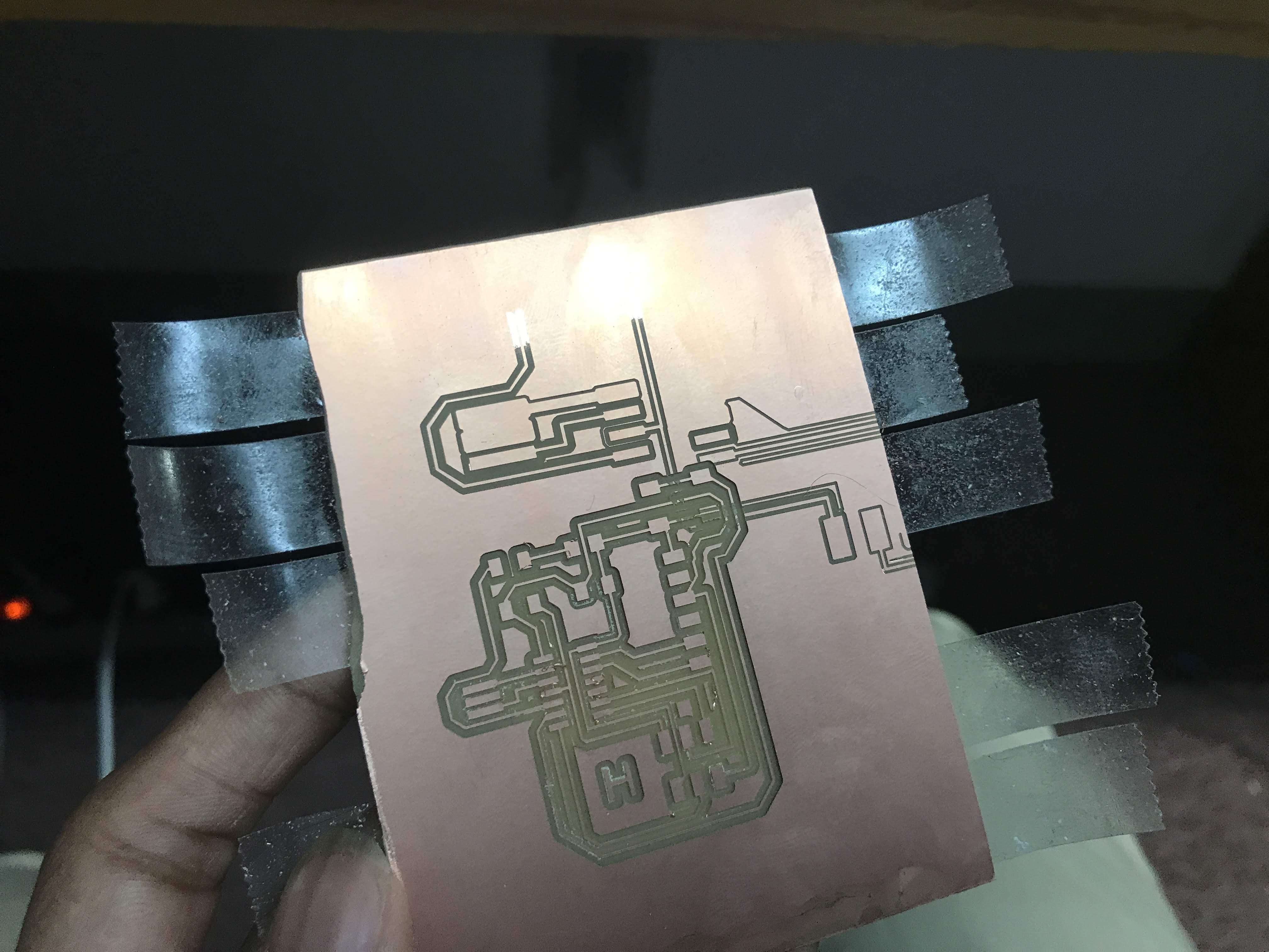
The first cut failed because I didn't tape it down hard enough, and the copper peice just came off.
The second cut failed because the copper was slightly bowed, and the mill bit was only carving the middle part of the piece.
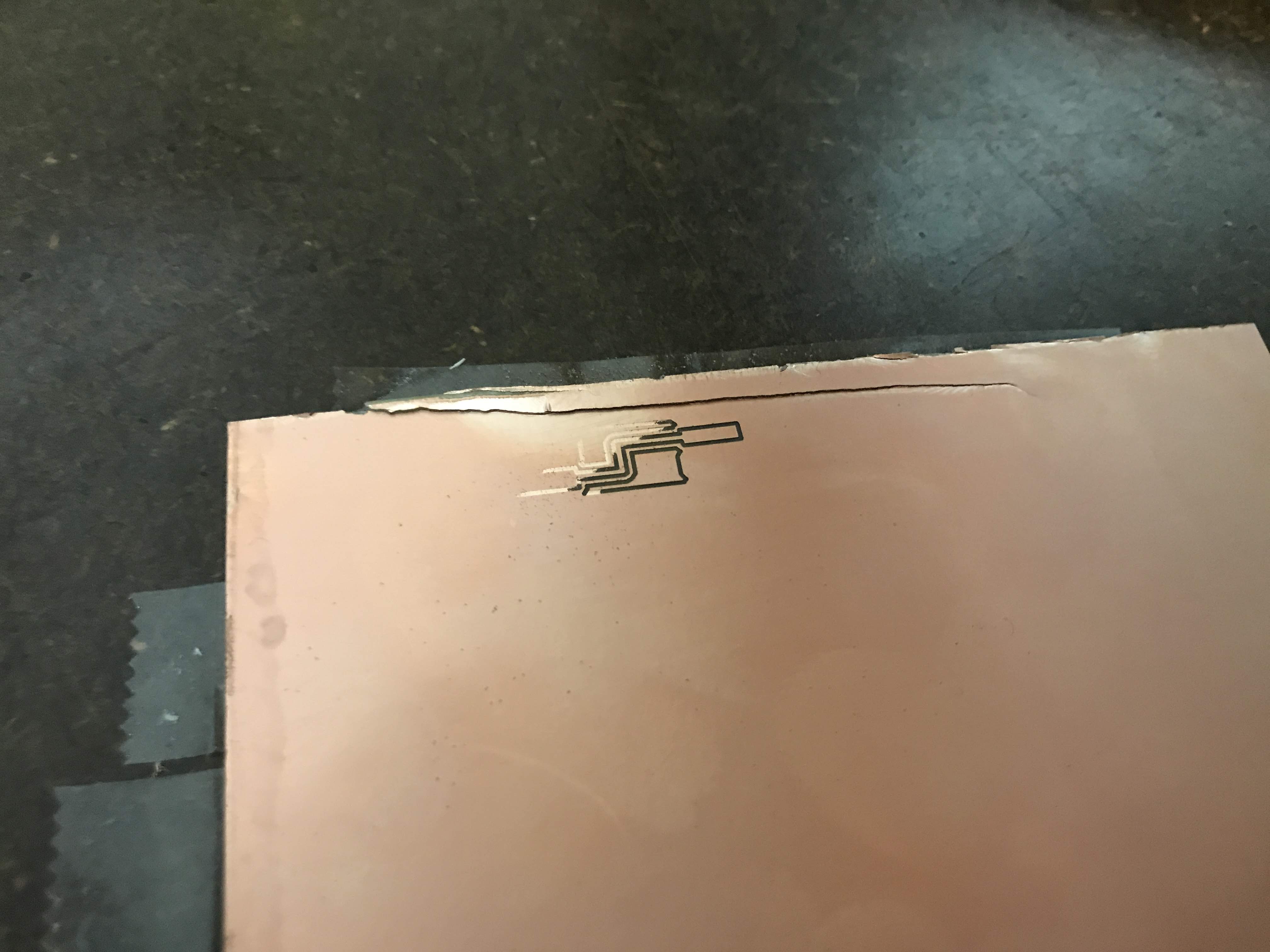
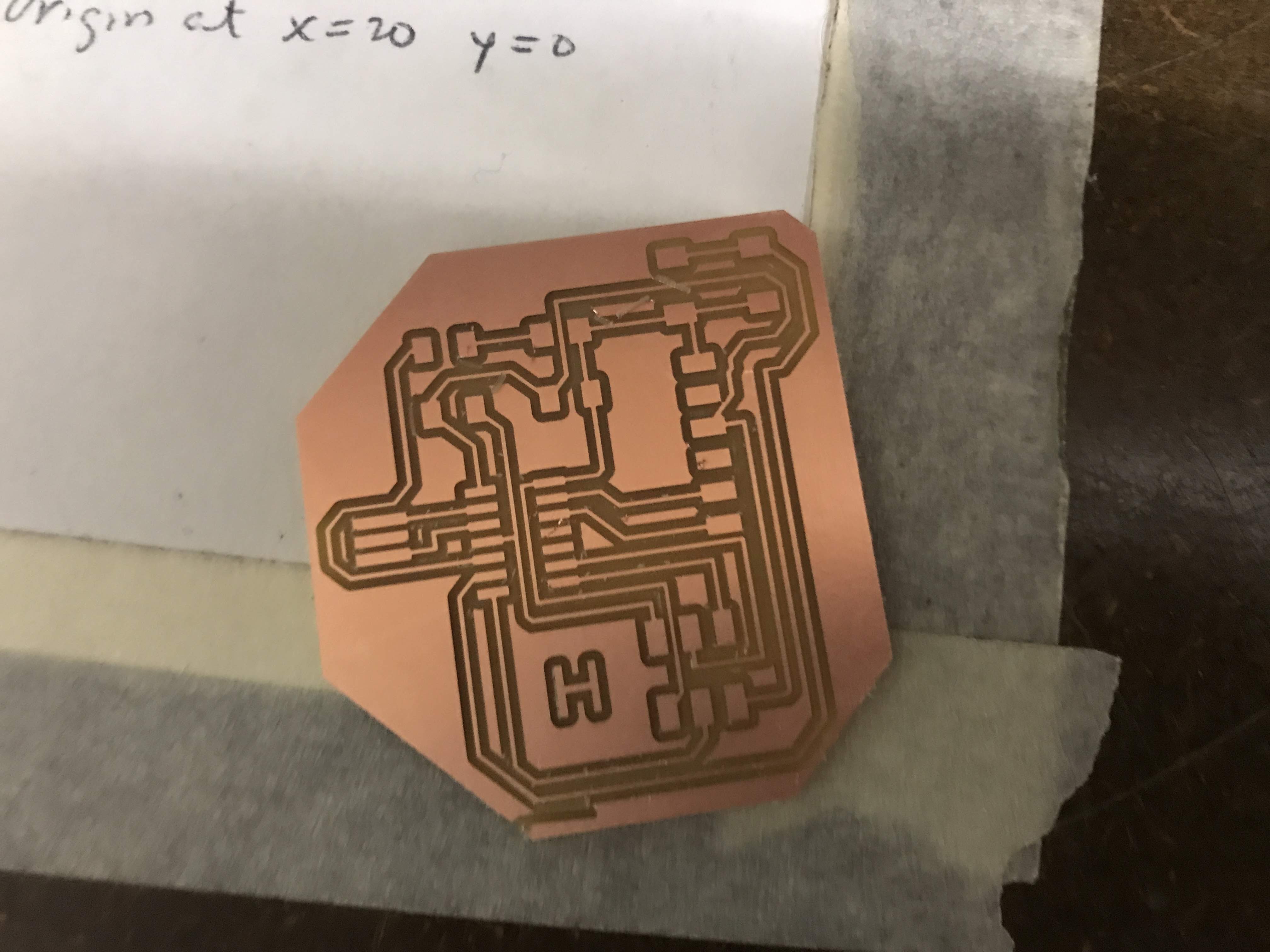
With the third cut, it started well, before the bit started moving off of the copper. I saw that the scale for the image was doubled for some reason! I'm not sure why this happened, but I doubled the DPI value, and it fixed itself from there. Wierd though, because I exported the PNG at 500 DPI, and initially had the setting set to 500 on MODS. In the below picture, you can see the first cut in the top left corner. I tried cutting over it, but the offsets made them run into eachother.
After that, the cut finally came out properly.
Soldering
Nothing new with this step. The soldering went smoothly!
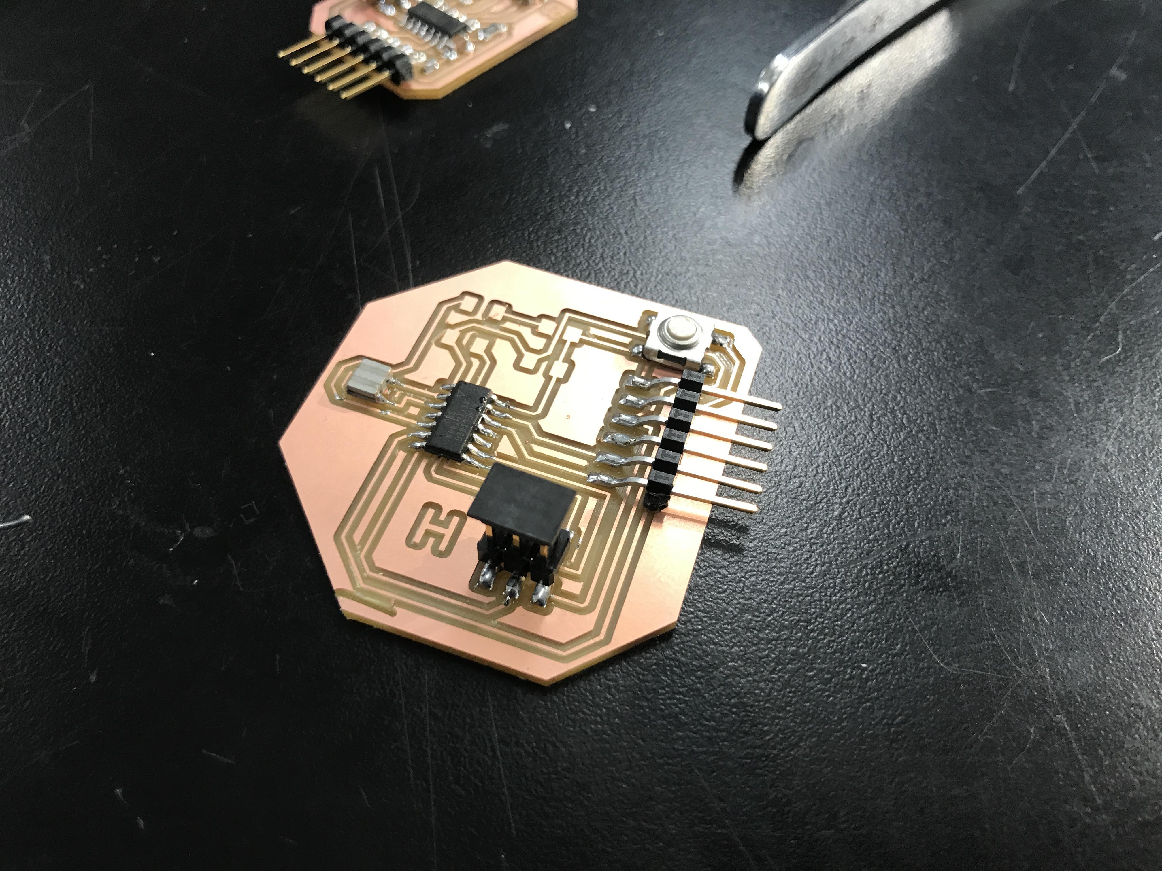
Well, until I found out that I had forgotten a ground connection to the 20mhz crystal. I didn't want to recut a new board, so I decided to solder a wire on top to connect everything together. Looks good!
