Week 3
Electronics
PCB Fabrication
Mill Testing
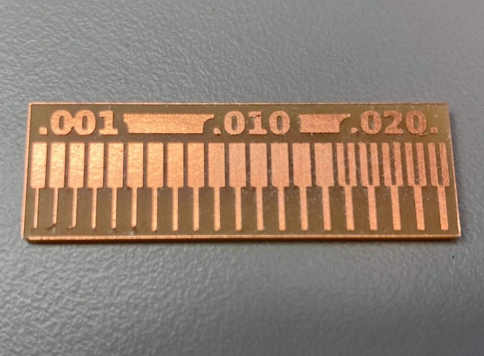
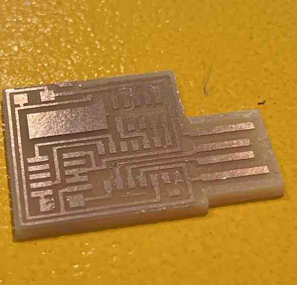
After completing the training for the different milling machines, we needed to run a test to ensure it is working correctly and the milling bit was in adequate shape. The bits wear down over time, which can lead to inconsistent traces and fraying of the copper.
To do this, we used this outline file for the exterior and this tracing file to produce the board to the left. After inspection, everything looked clean and consistent (completed on Roland Milling machine in EDS).
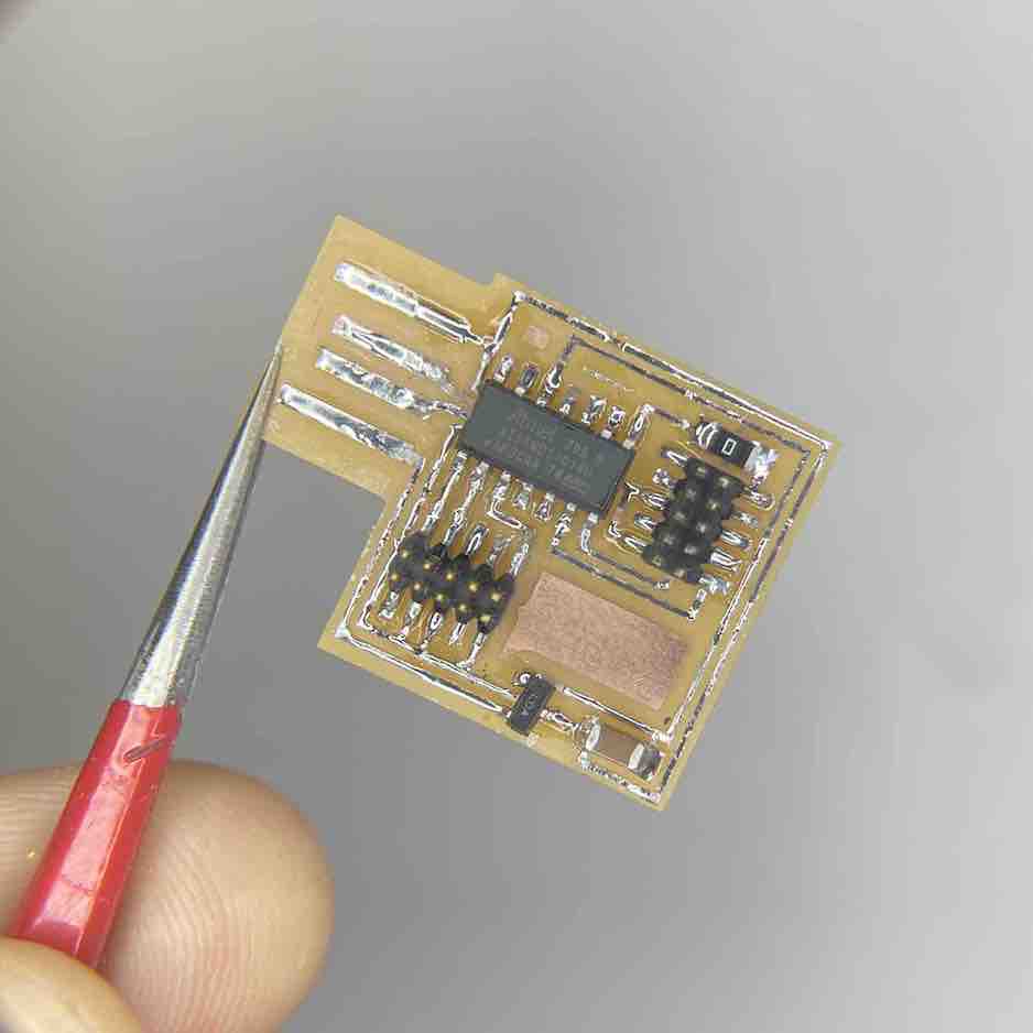
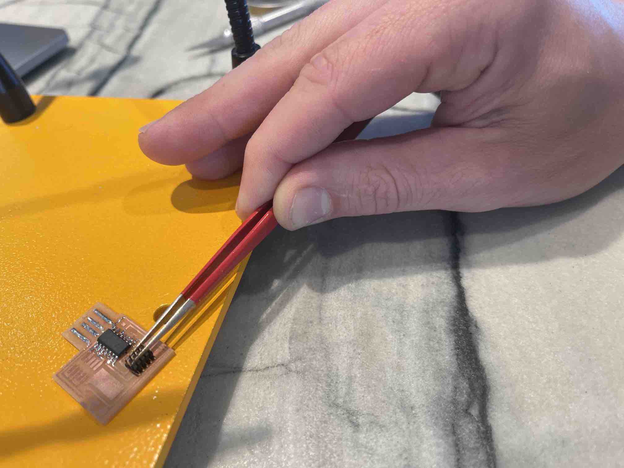
After the test, I proceeded to the weekly assignment, making an in-circuit programmer that will be used to program other boards (great example of the fablab philosophy of creating an item that allows for efficient scalability).
For my board, I made the CMSIS-DAP.10.D11C. This was decided based on usefulness and availability of soldering components
 Example Image
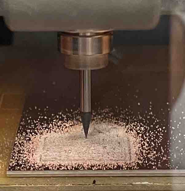
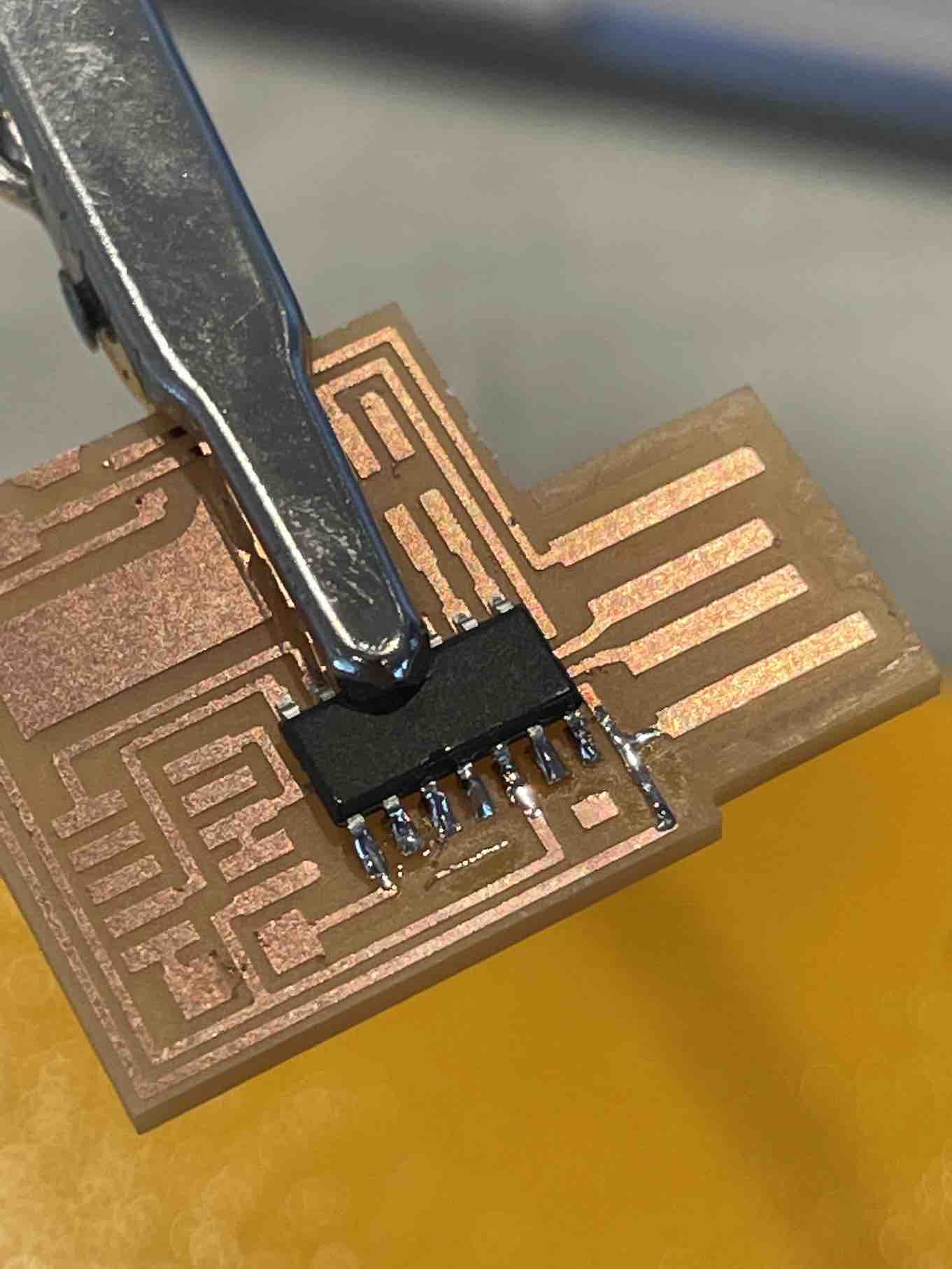
To mill this board, again we used the following vector files on the Roland milling machine, same as the test (Outline & Trace).
Some things to note are the different bits used. Fo the traces (interior) we used a 1/64" bit because of the fine spacing between traces. For the outline (and cut out) we used a 1/32" bit. You can use a 1/64", but it would be an inefficient process and dull the tool.
After milling the board, it was inspected the same way we did the test and no issues were found. It is best to do this next to the traces vector to ensure you are matching the intended pattern.
Soldering
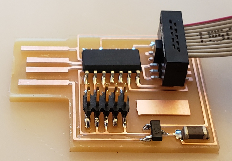
After the milling the components needed to be soldered on. A list of the components can be found on this diagram.
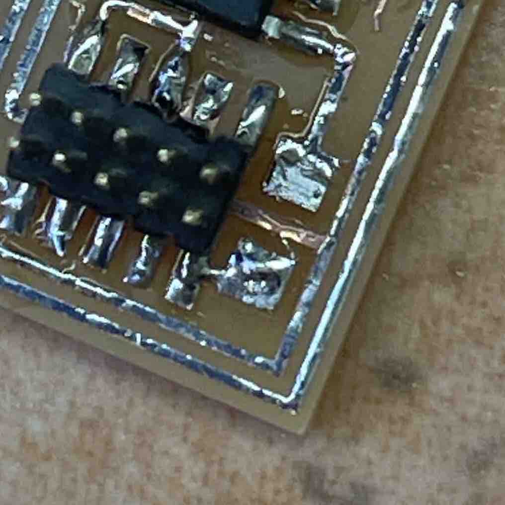
For soldering, there were a few tips I found particularly useful.
- Heating up the intended area is critical. If the solder doesn't flow instantly, you didn't warm it up enough. Furthermore, use a wider soldering tip that you think. This will help heat transfer and you still have dexterity.
- Use lead based solder. You can use non-lead based, but it doesn't flow nearly as well. My previous experience has been with non-lead based, I didn't realize the difference would be so significant.
- Anchor your hands, especially with tweezers. By extending the pinky and placing the base on the palm on the table, I can mitigate issues with shaking.
- If you need to remove excess solder, it's easier to draw it down traces than to remove. This is also helpful because it prevent corrosion.
Once the soldering was complete, I needed to test the board. This was a quick exercise with the help of our TA, Anthony. I don't have full understanding of the exact steps yet, but the strategy is simple. When you don't have insight, you test connections for electrical flow. Sometimes you are testing to make sure it isn't present, other times you are making sure it is.
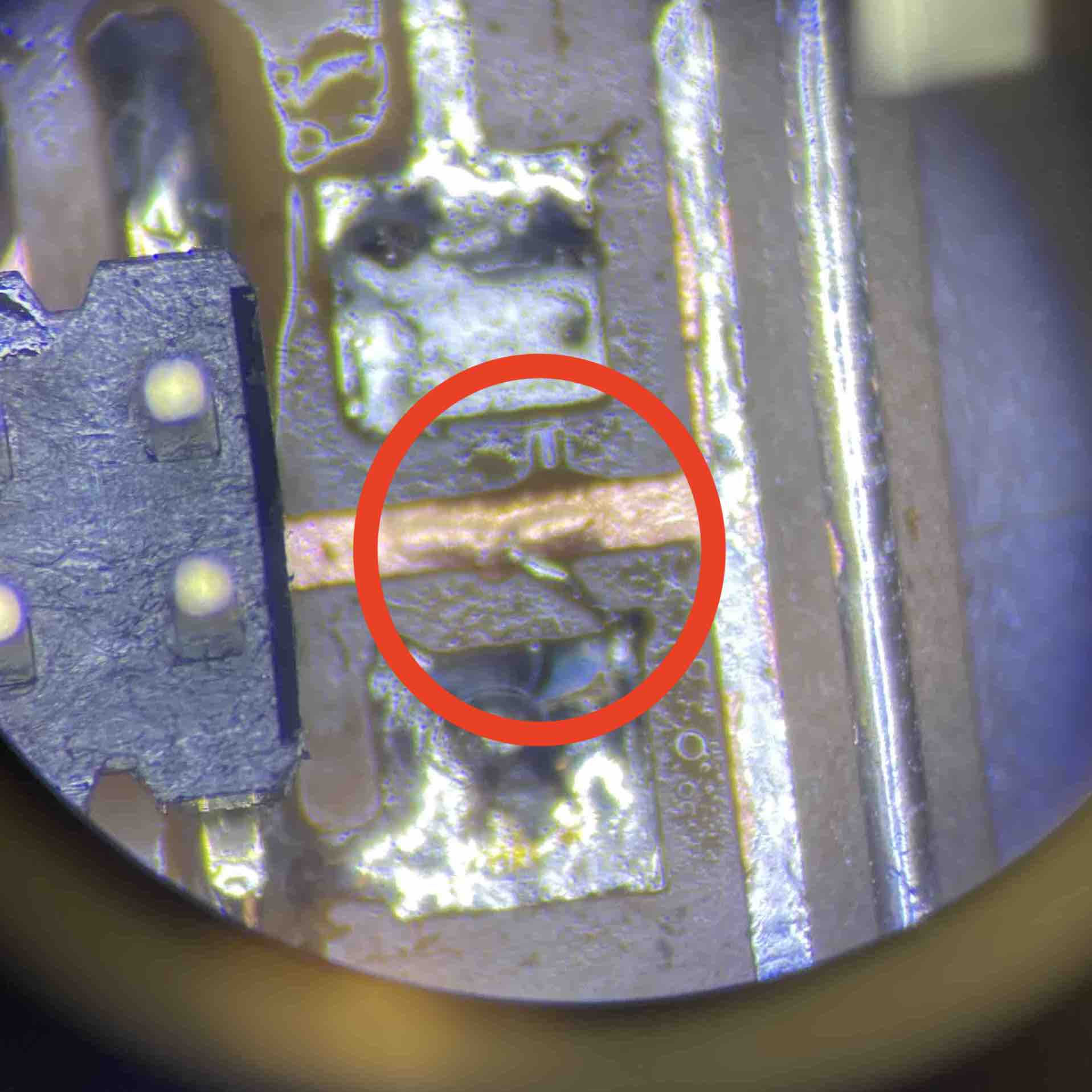
If you do find one where it shouldn't exist, solder is probably making a wrong connection. This is what happened to me.
I heated the solder to remove the component and saw the issue. I couldn't tell at first with my naked eye (top picture), but the issue was obvious under the microscope (bottom picture). This shows the value of assistive vision.
In addition to fixing the soldering error, I thickened the USB connections by layering soldering on the traces. My best advice here is to do more than you think. That lift will improve USB connections and make future work more seamless.