Week 5: Electronics Design
Goal: Redraw an echo hello-world board, add atleast a button and an LED, check the design rules, make it, and test that it communicates.
Group Project
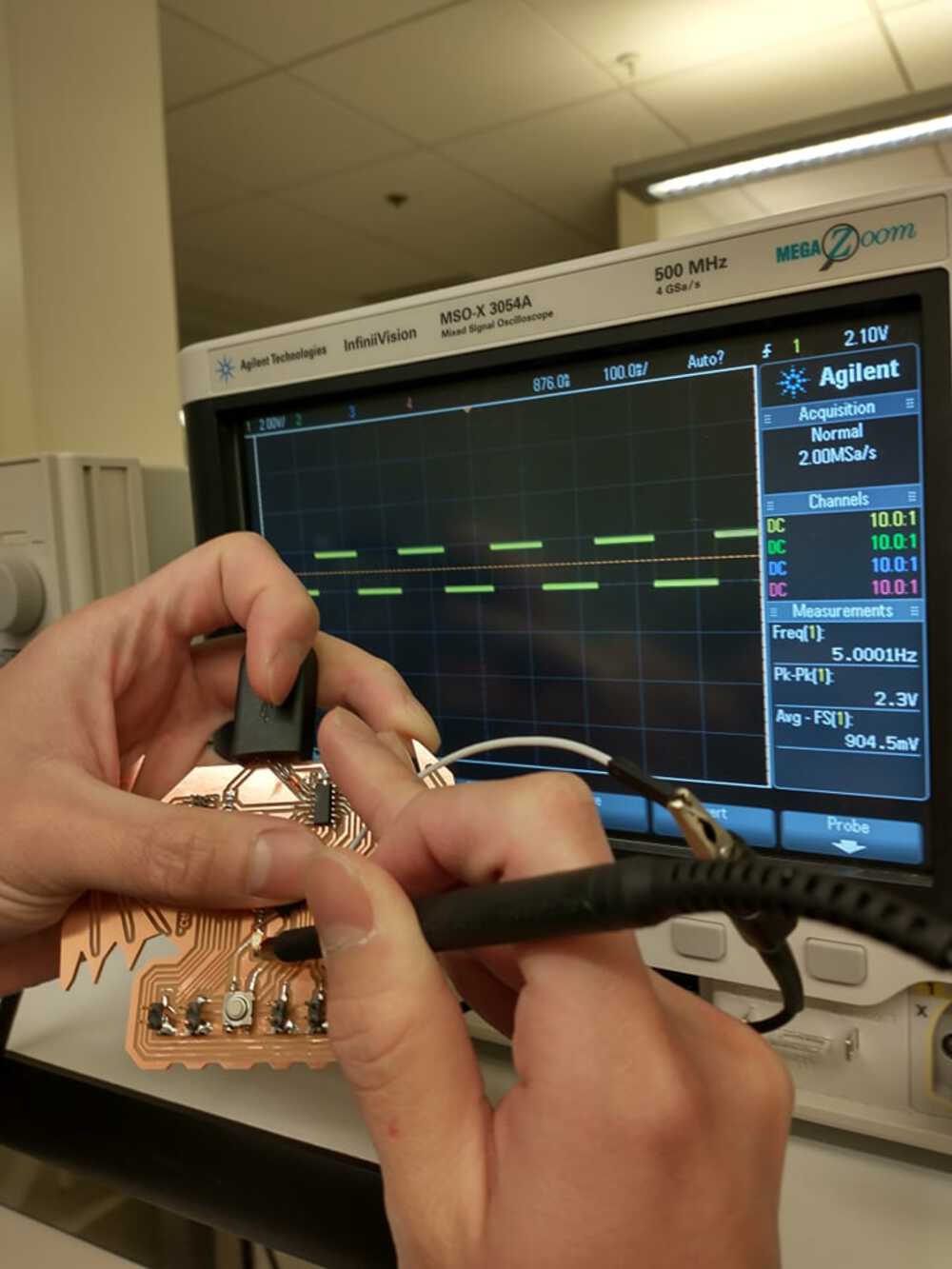
This week's group project was to use the test equipment in the lab to observe the operation of a microcontroller circuit board. To do this, our group used one of the oscilloscopes in the lab to measure between the 3.3V pin of the LED and GND. On the screen we were able to see alternating high and low volatages which lined up with our expectation. The program we were running consisted of turning the LED on, waiting 100ms, turning the LED off, waiting 100ms, ... over and over. We were able to look at the frequency of the alternating high and low voltages to see that they were alternating at a frequency of about 5Hz which was expected given the on-off cycle of 200ms we hardcoded. Below a photo of the oscilloscope reading out the different voltage featuring Ben's board which was used for the test.
Designing in Eagle
This week I choose to re-design the ATSAMD11C hello.D11C.echo board using Eagle since it comes prepackaged within Fusion 360 which is the CAD tool I decided to learn in previous weeks. The process of designing started off pretty rough when I could not get the FAB library with our components loaded into the software for use in my design. However, Anthony helped a couple of us debug this issue and was able to figure out that for some reason Fusion 360 only loaded half the library the first time you uploaded it to the library manager. Thus we were able to try adding it twice with different names and it ended up adding different halfs each time so we were left with the whole library! Success! Once that was out of the way, the process consisted of:
Design Images
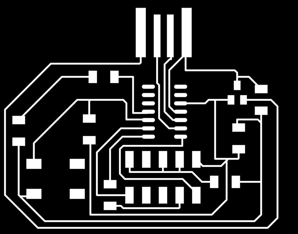
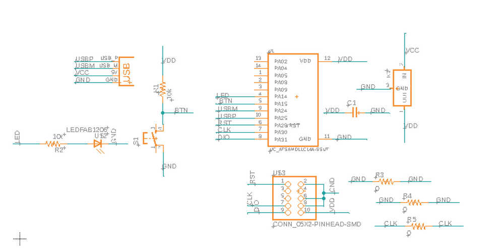
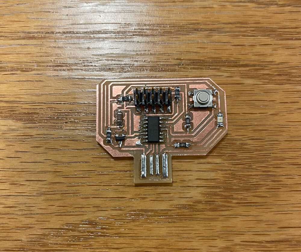
These are the schematic and board designs I ended up with. In retrospect I probably could have spent some more time on the routing to use less jumpers, but overall it looks ok.
Milling
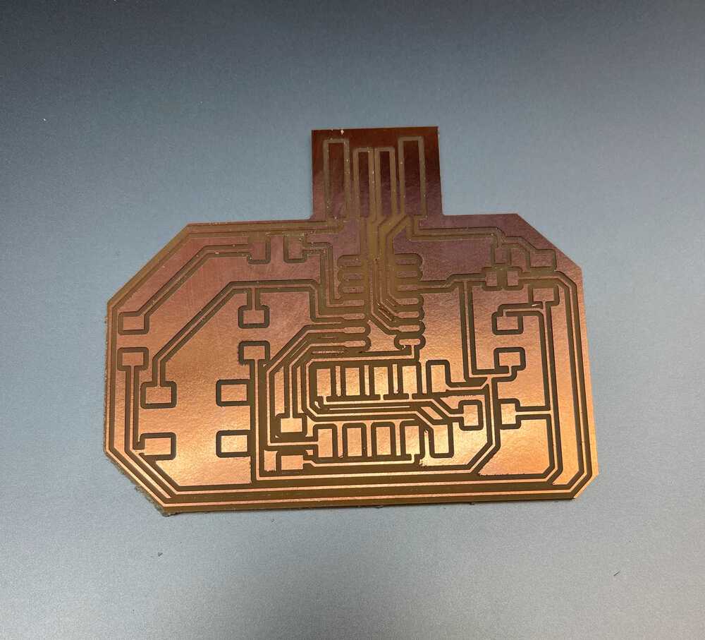
Milling this week was much more of a struggle than last time we were assigned to mill a board. On my first attempt, I discovered the weird bug on mac with eagle that halves the dpi (doubles the size) and unfortunately printed out a massive board. Luckily I had the time to go back into lab the next day and re-mill another board with the correct dimensions. On my second attempt, however, I ran into significant burring so before soldering I spent some time with a spackle knife making sure my traces were cleana and shiny.
Soldering
After many messups in week 3 involving trips to the heat gun to remove components, I was determined this week to do better with my soldering. I figured out that in week 3 I was spending way too little time heating up the component and copper before trying to add the solder and that was causing the solder to just attach to the soldering iron and not the board and component. This week I took my time and made sure the component and copper were adequately heated and I had a much easier time getting better solder joints.
Programming and Testing
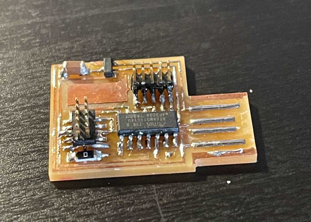
In order to program and test my board I used the programming I made in week 3 and tried bootloading the board I made this week from my mac with EDBG. In this process I ran into two problems. First, my programming had a faulty solder joint where no current was passing through. Anthony showed me on the multimeter that communication between pin 2 on the microcontroller and the programming head was not happeneing and that I needed to go in and add more solder. It is hard to see in the photo, but the second pin starting from the right does not have much solder underneath the leg connecting to pin 2. The second problem I ran into was actually using EDBG from my mac. I was able to download it using "brew install edbg" however when trying to run the command "edbg -b -t samd11 -pv -f sam_ba_Generic_D11C14A_SAMD11C14A.bin" I received the error "Error: invalid response received". Due to time constraints I was not able to try using pyocd or openocd which I was told could serve the same function as EDBG, but in later weeks I hope to get this working on my own computer so I don't have to go into lab in order to bootload a microcontroller. Luckily, Anthony was there to save the day again and we were able to bootload the microcontroller from his computer using the same commands!
Flashing the LED
With more help from Anthony we loaded up a test programming using the Arduino IDE and were able to successfully flash the LED on and off!