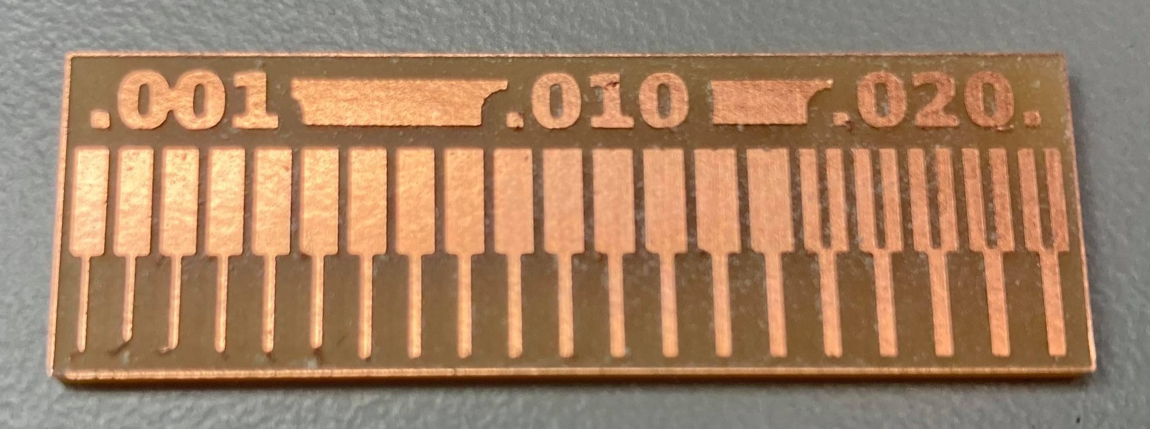
As electricity can run through extremely thin pieces of metal, trace size is dependent on machine capabilities, so this characterization demonstrated how thinly the mill can reliably create traces for. As the file wasn't unable to run on the Othermill, despite lengthy troubleshooting efforts, our section was only able to run this test on the Roland. Trace width starts getting unreliable once thinner than 0.010 in.
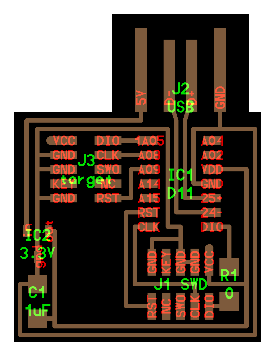
Anthony and Harrison recommended milling and soldering the FREE-DAP hello.CMSIS.DAP.10.D11C board, now called the USB-D11C-SWD-10. (The other PCB typically recommended for this week required a component that is currently out of stock due to price spikes from COVID-19.) I decided to use the Othermill for a few reasons. Although its milling time is longer than the Roland's, the Othermill is a bit more straightforward to use, as the software calibrates the z-axis on its own and simultaneously loads both the trace and outline designs. Additionally, I also wanted to begin familiarizing myself with the Othermill first, in case I wanted to mill double-sided boards in the future, which the Roland cannot do.
How to Othermill:
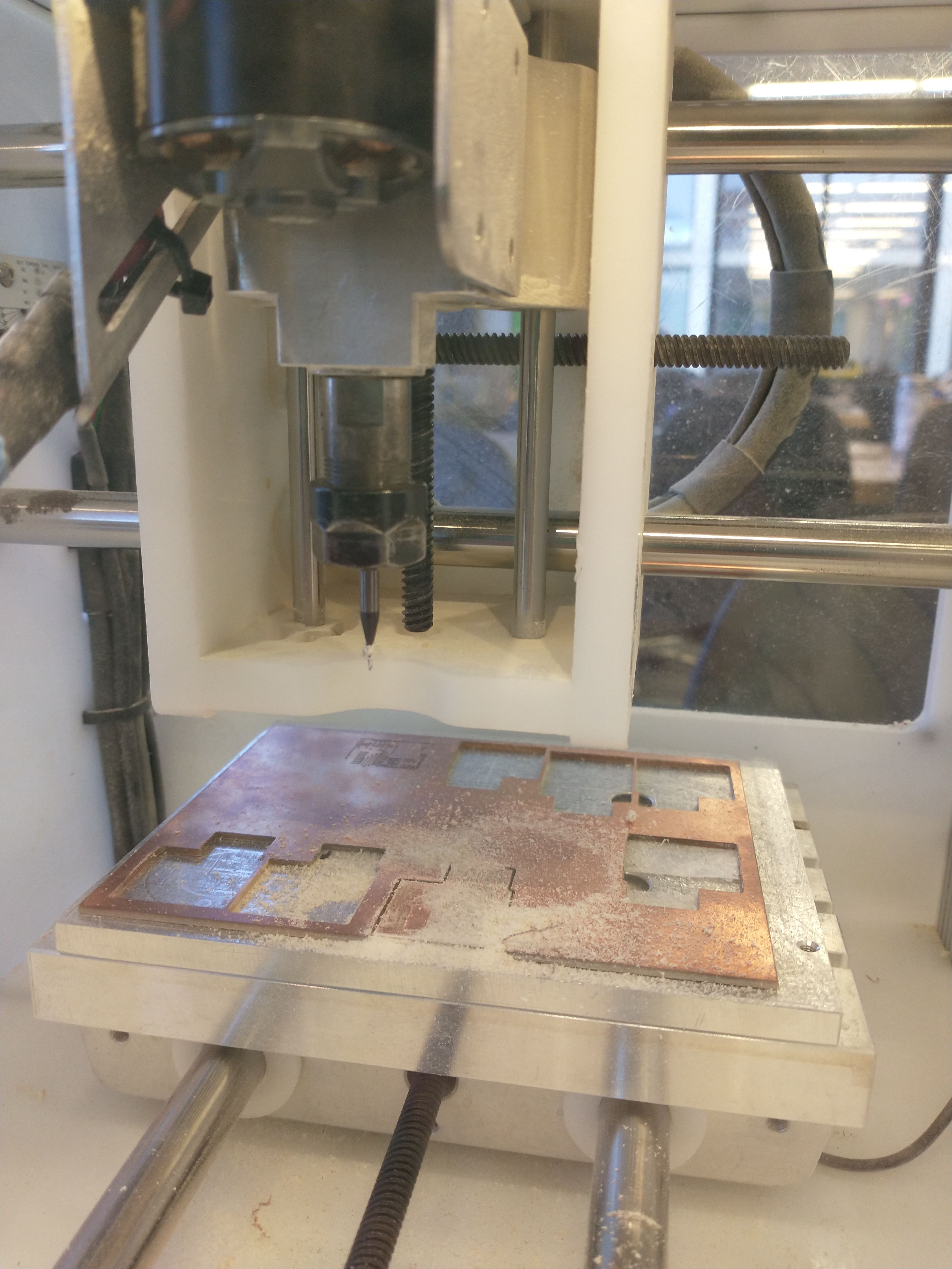
This board took about 20 minutes to mill. For some reason, after switching from the 1/64 flat end mill to the 1/32 PCB conservative tool, the machine did not automatically begin milling again, so I cancelled the job, removed the 1/64 tool from the list of tools, and did the 1/32 milling as a separate job. Sandpaper is handy for cleaning up the burrs, especially since the brush I first used seemed to have little to no effect. Cutting the copper off from the USB insertion took a while, as the copper refused to peel, so I used an exacto knife and a box cutter to scrape it away.
I had to mill a second board, since one of the traces on my first board became damaged while I was prying it off the bed of the machine; I used the first board to to practice soldering and the effectiveness of the sandpaper. I also learned to be very distrustful of any z-axis movement and the mouse's ability to control it.

The Othermill uses a stepper motor, which is also used in 3D printers. Its sound at the start of the milling process, in my opinion, sounds like the opening to Carmina Burana.
Some general tips for surface mount soldering: Solder all leads of a part, even if they aren't used. Regarding the soldering iron, tip shape more important than tip size; get a cone with two flats on it, and set the temperature to 750 degrees F. Touch the soldering iron to both the lead and the copper trace. Tack down parts by putting solder on a pad then aligning the part with the rest of the pads. Solder parts bottom to top, inside to outside, smallest to largest. Inspect carefully under the microscope for any issues. If trying to remove solder, pull the wire and iron away at same time. Since we're using leaded solder, solder in big open areas, use a vent, and wash hands afterwards. Solder is actually hollow, since there's flux in the middle, which is a mild acid that helps with heat transfer.
If using solder paste, wear gloves. Clamp the board, paste all the pads, place all the parts, and heat everything at once. Anthony uses 330 degrees Celsius and recommends 270-330 degrees (or lower if you prefer to work slower). Reflow ovens result in a loss of temperature control.
Parts
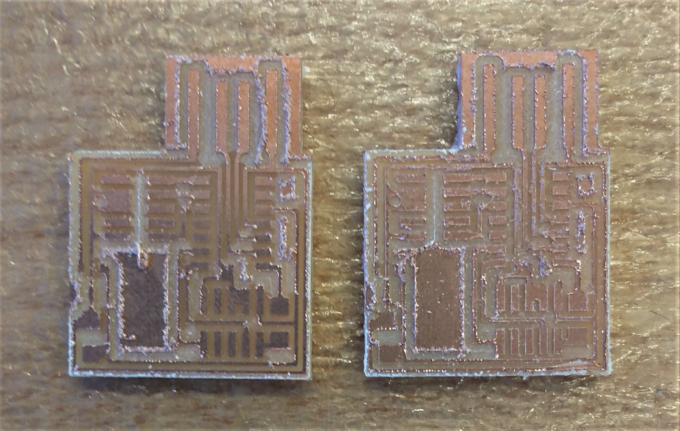
Soldering went rather smoothly, sans burns. For the USB port, Anthony recommended putting solder on the USB traces by keeping the entire section of solder hot so it solidifies evenly. I'm also quite glad I stripped the copper from the USB before soldering, as the parts would have just gotten in the way.
From Anthony's soldering demo, starting from the smallest components definitel makes the process easier. I also should have done the larger flat components before the larger spikier ones, as manuevering around the extra height was a tad annoying. I would still like to learn how to solder without creating spikes when the iron is pulled away. I was surprised to find just how much fine motor control that soldering required, especially for the smallest components - the capacitor and resistor. I tried using a clamp to hold my board in place and ended up optiming to use a piece of double-sided tape.
In two areas, the solder for two component leads ended up getting fused together. Since these leads were connected anyway by the traces, there was no need to fix this. Viewing under the microscope showed that there was an excess bit of copper that had to be pulled away with tweezers; it had snagged a bit of solder and was a bit too close to comfort to another trace. Finally, I added vinyl to the base of the PCB for extra height, which is Neil's preferred method of maintaining a good USB connection.

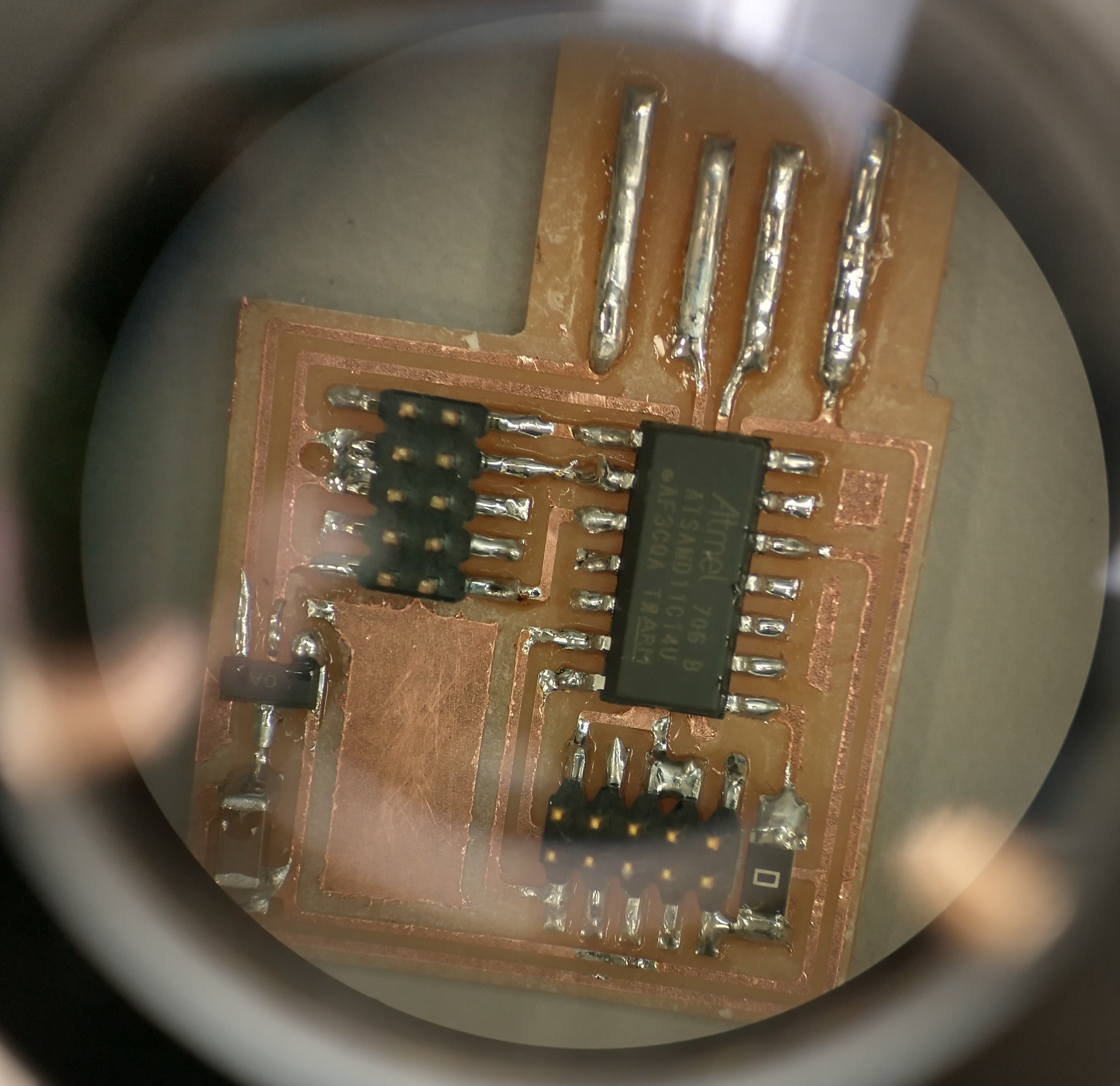
I even managed to snag a decent photo through the microscope! Bootloading and testing the PCB worked succesfully, though it took two attempts; what appeared to be a computer was in fact merely serving as a computer stand and thus could not connect to my board.

Thanks to Harrison and Anthony for their assistance this week, and especially to Anthony for his extremely helpful electronics primer! "If you think something is broken, hit it with a hammer and then it's definitely broken" - Anthony Pennes, 2021