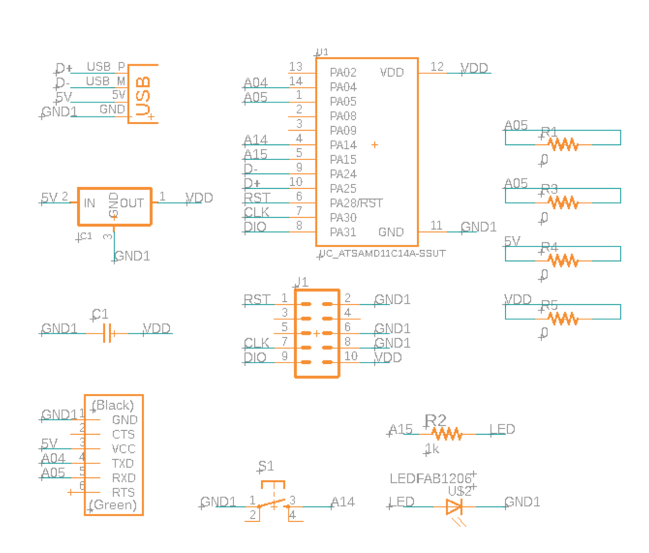

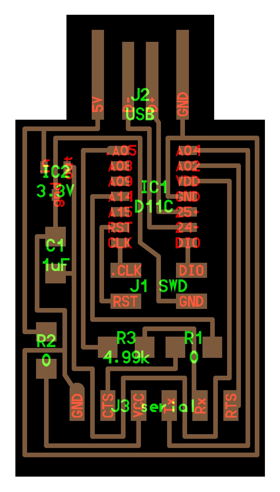
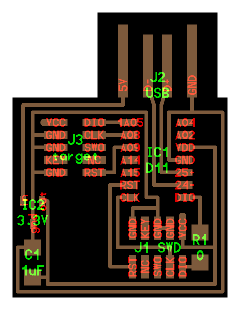
Anthony recommended that I build my board design off of Neil's hello.D11C.serial.5V.1.1 board and to replace J1 SWD with a 2x5 pin connector that I used in Week 3's hello.CMSIS-DAP.10.D11C board.
I opted to use Eagle, since I already had Fusion, wasn't thrilled by KiCAD's UI, and have heard Harrison and Anthony mentioned over the weeks. The standalone Eagle software installed but failed to load despite troubleshooting, so I just used Fusion Eagle instead, which had its own delightful set of UI annoyances. Most notably, both schematic and board files (and their container file) have to be open simultaneously. Making changes with just the schematic file open results in error messages, as well as failed attempts at ERCs and synchronization. The solution is to just undo all the changes made earlier and reopen all the files. Another UI feature that bothered me was the process of moving parts, as you have to find the origin of the part (usually indicated by a X, usually hidden and/or resembling another aspect of the part) in order to click and drag the part.
Step 1 was to locate all the parts I wanted to use in the fab library. For future reference, the wonderfully unintuitive names of all the parts I used are as follows. Parentheses indicate subfolder names.
I referenced Neil's board designs (linked above) to determine which pins should be connected together, using the Week 3 board as reference for the connections for the 2x5 connector, which had 3 GND pins and pin 10 connected to VDD (3.3V). Pin numbering for microcontroller involves count the pins counterclockwise starting from top left. For the 2x5 connector, pins are numbered left to right, top to bottom.
Handy Eagle Tips (thank you Anthony)! The software will automatically connect wires for you if you drawing short wires from each pin and then name the connecting wires with the same name (I usually named them based on where the wire is going - i.e. a particular pin on the microcontroller or parts of the USB port). Naming wires GND automatically connects it to a GND pin (in my case, the one on the microcontroller), so I opted to name the ground wires GND1 just to be more methodical about connecting everything myself and being able to label everything. The order of the parts does not matter in the schematic (unless parts are connected in series). Renaming wires just involves selecting the "Change name of every segment on sheet" option.
To add the LED and button, I referenced Page 8 of the SAMD11C microcontroller datasheet, which indicates which pins are digital and which are analog. For the purposes of this board, it didn't matter which kind I connected the LED and button to, so I just chose digital, especially since those were the pins that weren't already wired to something.
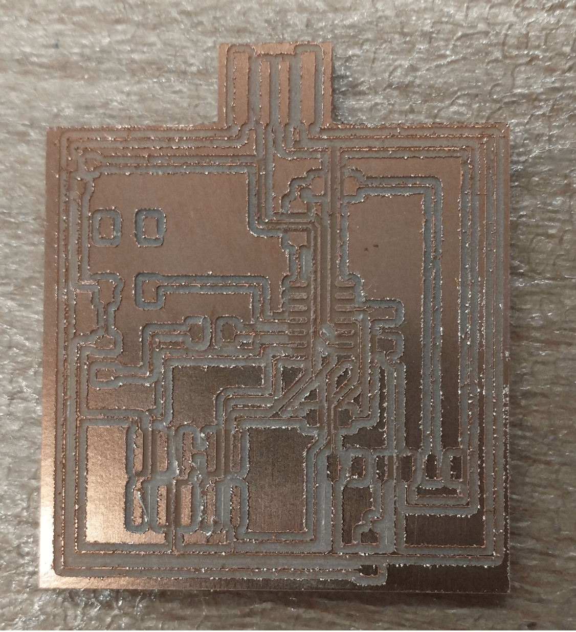
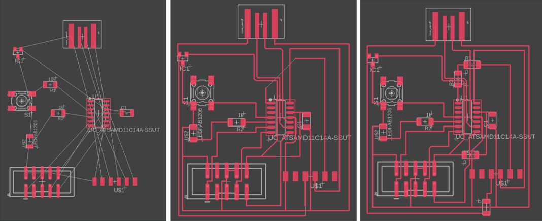
When it came to drawing traces, I just decided to go for it and mess around from scratch, instead of copying from a reference. The first step was placing all the parts on the board with the least amount of crossovers between the parts. I placed the voltage regulator in the top left of the board, given its USB connection. To connect the D+ and D- USB traces with some of the microcontroller pins, these traces went underneath the microcontroller, which can fortunately fit a total of three traces. For future board designs, I should prioritize these traces first. I also placed the capacitor as close to the microcontroller as possible, since its purpose is to provide the microcontroller with charge if there's a sudden demand.
Rotating objects also helps out with the process. The alt key allows for more precise grid snapping. The default grid was more course and resulted in some angles in my traces and some wobbled lines, which I cleaned up at the end.
Notes on Settings: Set trace width as 10. Ffor DRCs (design rule check), under Clearance, set all the top values (wire, pad, via) to 16.
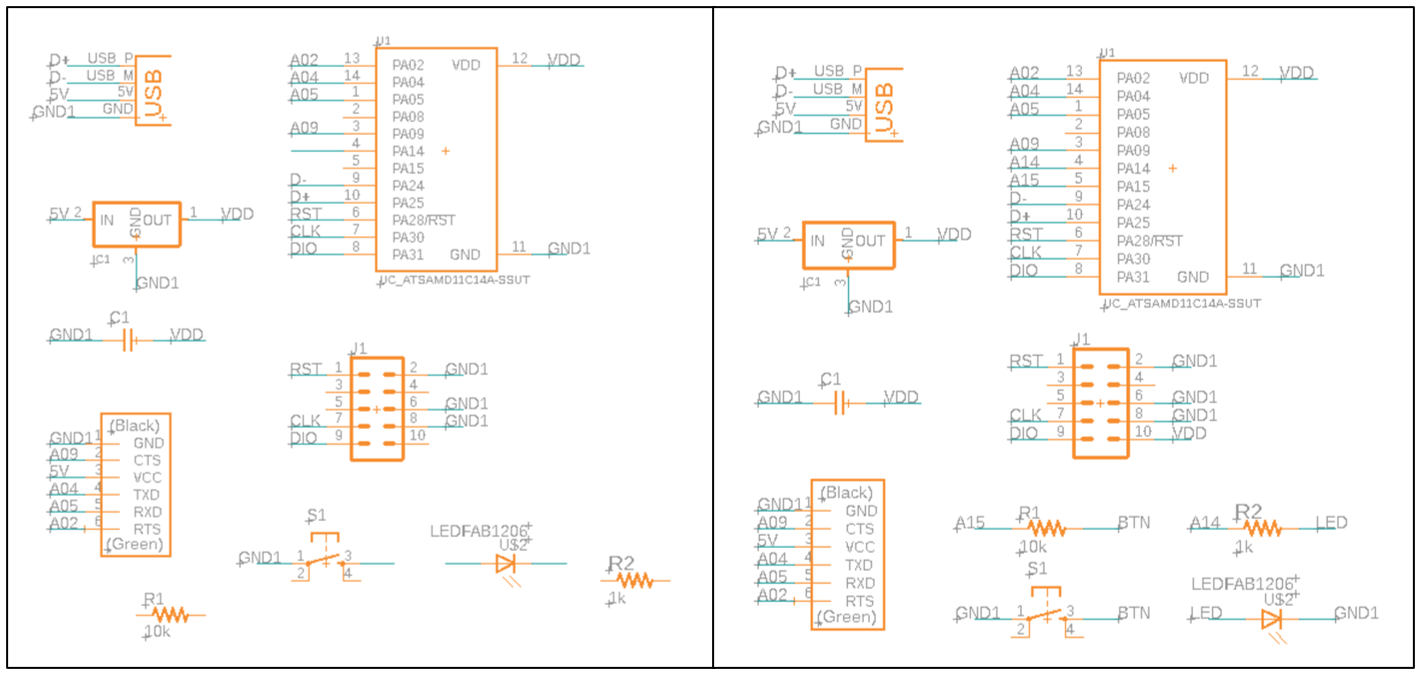
I made a few modifications to my schematic during the board design process. I swapped the pins that the LED and button were originally connected to, to reduce overlapping wires. I deleted the CTS and RTS connections to the microcontroller, since Anthony mentioned that we won't need them unless we are processing very large amounts of data. I also deleted the 10k resister by the LED since I accidentally connected it in series with the LED and microcontroller and because there is already a pullup resistor built in, though I'd need to program it in. Since a few bridges across traces were needed, I grouped together some traces and added four 0 Ohm resistors in my schematic.
Board outline notes for the future: Be sure to draw the outline of the board exactly along the USB out1ine, and leave some space between your traces and the edge of your board, in case the milling tool's activity results in unexpected dimension changes. (Thank you Solomon for letting me know the importance of this, thank you to last night's me for defaulting to doing this).
Schematic and board design files can be found here.
Eagle exports the file as a .brd, which can be directly opened with Bantam Tools for the Othermill, which meant I didn't have to use mods. Milling went fairly smoothly, especially since I just had to reference my notes on the process during Week 3. The only issue that I ran into was that I underestimated the size of my board, and someone had already engraved part of the material that my board would have overlapped with. I realized this after the 1/64 endmill finished its couple of minutes of milling, so I just swapped the material out with a fresh piece and restarted the milling process.
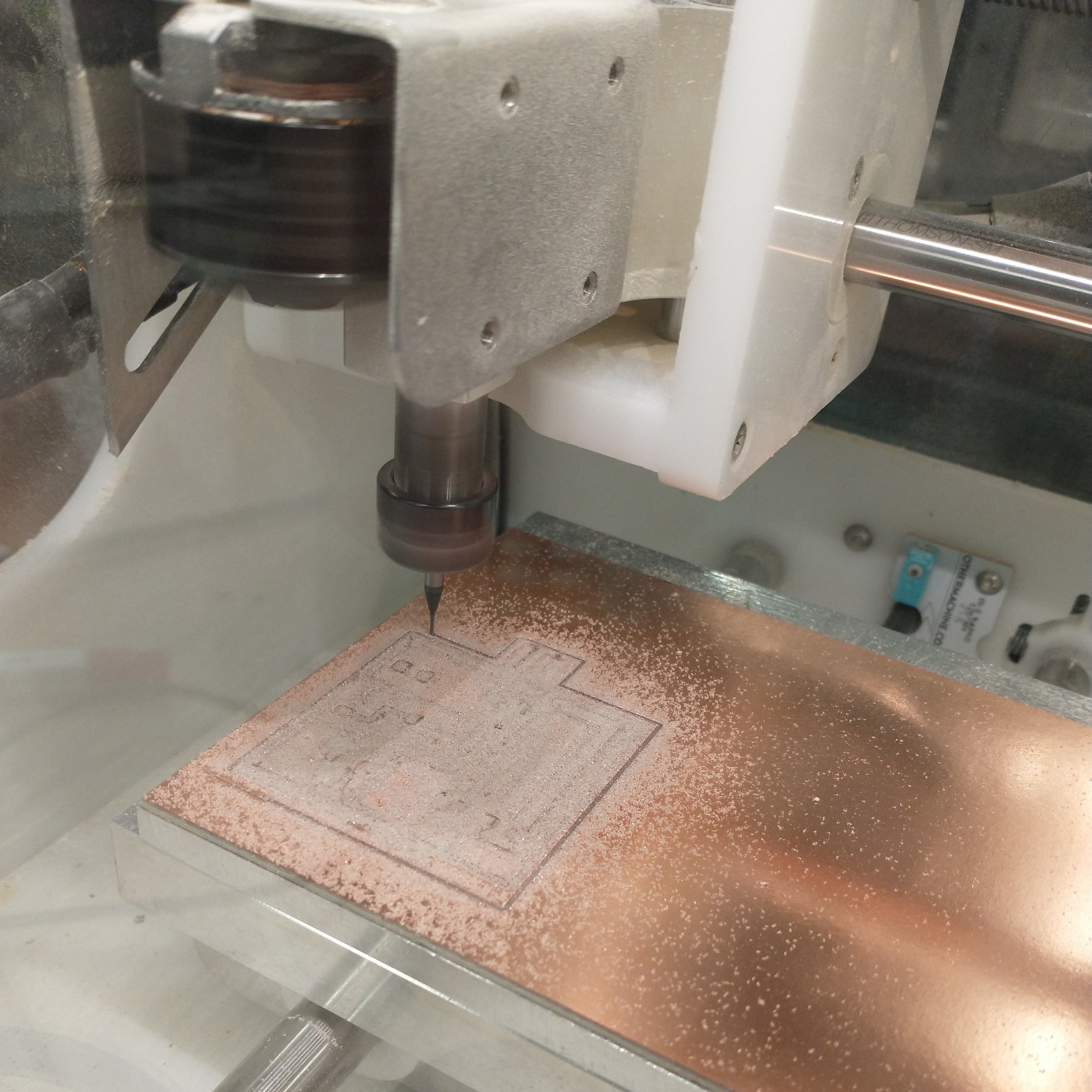
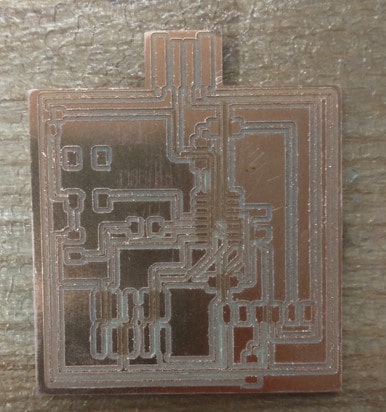
After swapping out the tool, you just have make sure that the window is closed before you do the z-axis calibration process. This prevents the machine from not actually restarting the job after the tool change, which was something I experienced last time. After milling, the board was covered by a good amount of burrs, so I sandpapered the entire board and of course removed the copper around the edges of the USB port (once again, before soldering).
Locating parts was a fun adventure. It turns out that the 2x5 connector in the fab library is not the exact same one as the one I used in Week 3 and is in fact bigger, which EDS fortunately had in stock.
Parts
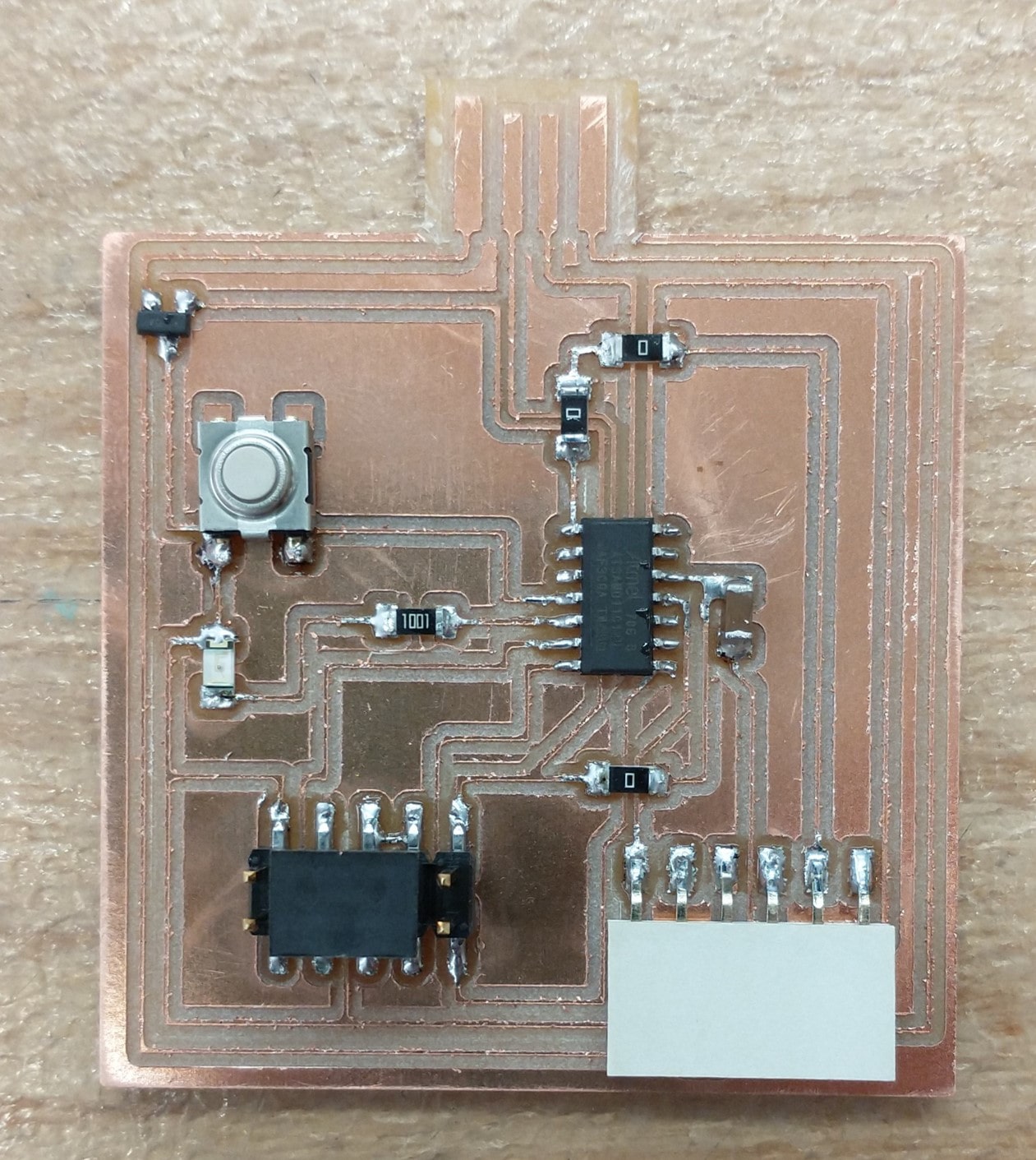
Soldering went fairly smoothly. I soldered all the small parts first roughly top to bottom, left to right, then did the same for the large parts. The only change I'd make would be to check the board under the microscope before soldering on the 1x6 connector
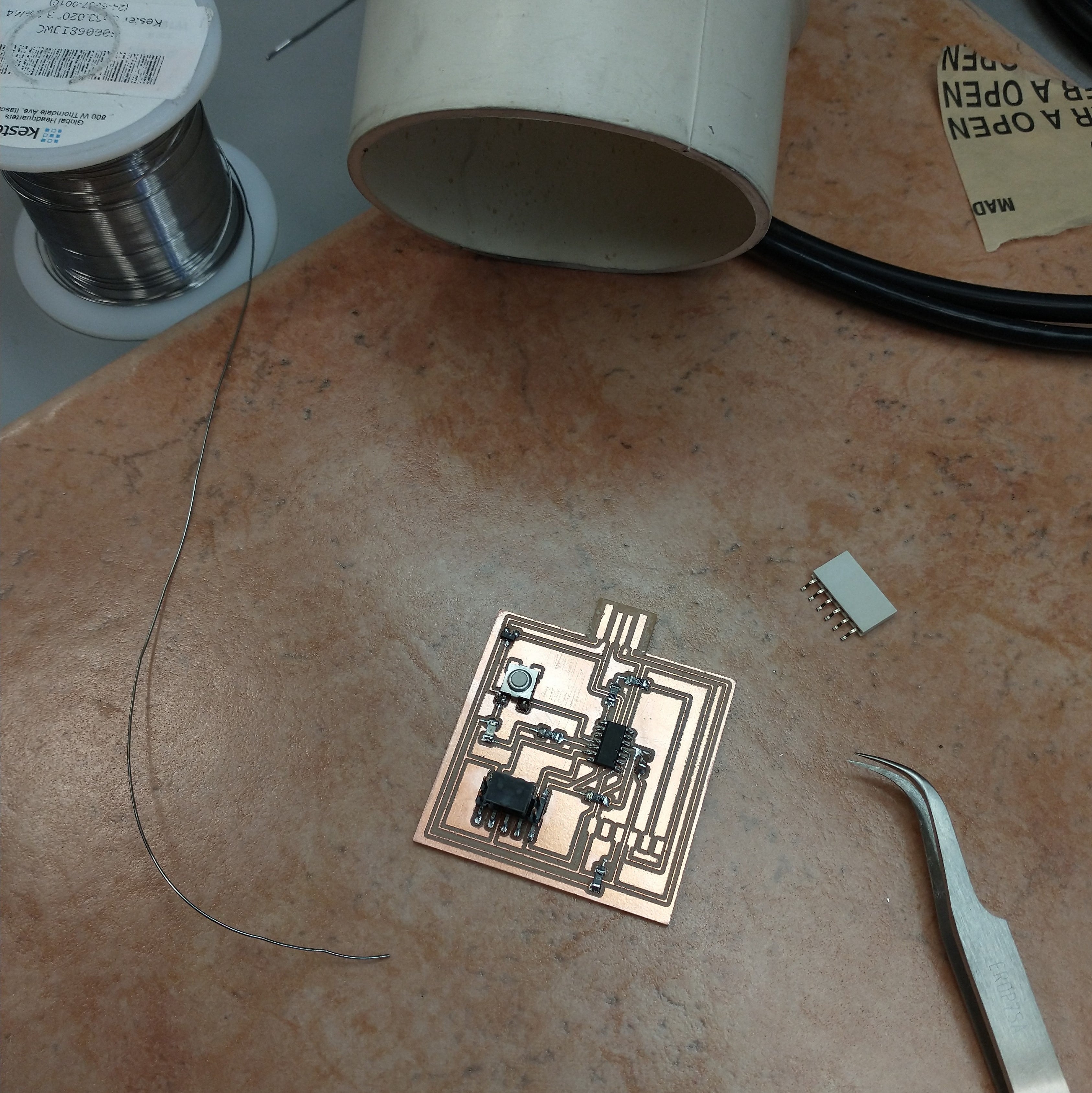
I added a few layers of vinyl underneath, since I didn't feel like soldering the USB port like last time, though I only need to coat the USB section of the board and not the bottom of the entire board.
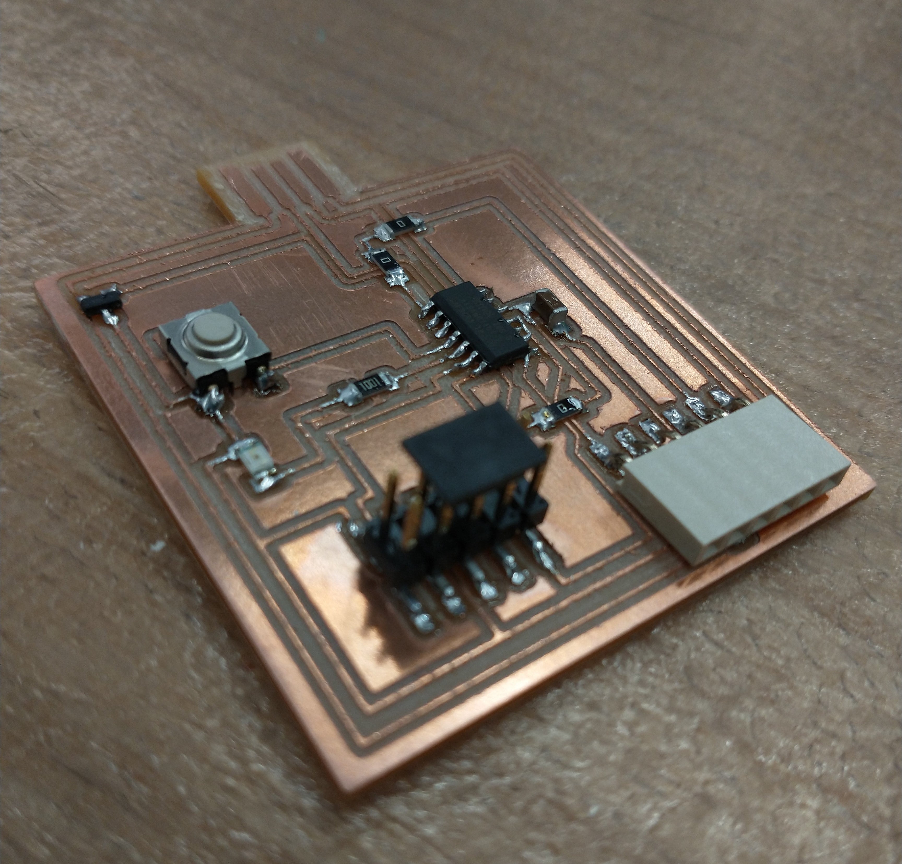
And here's the final product!
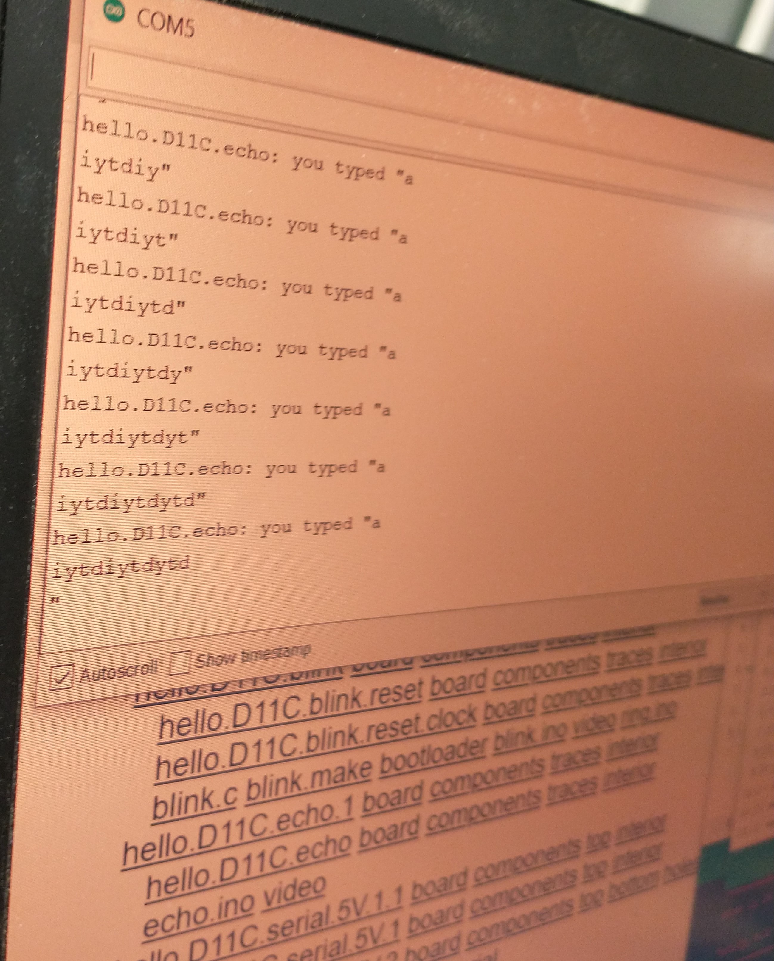
Anthony helped me bootload my board using an Atmel ICE and Microchip Studio. We received a device signature (which means we can program the board), uploaded a generic bootloader, verified that the receipient was in fact my board (since it shows up as a USB serial device under Ports), opted to upload echo.ino instead of blink code for reasons, and tested that the code worked properly by keyboard smashing.
The board works!
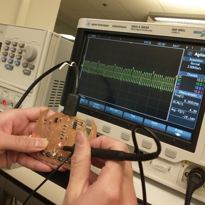
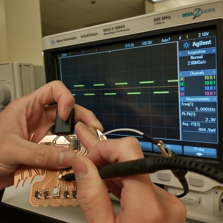
For the group assignment, Ben uploaded a short piece of code to his board to have his LED turn on for 100 milliseconds then off for 100 more. We used the oscilloscope to measure the signal and initially received a strange number for the frequency. Once we added a probe to measure the ground signal, the oscilloscope displayed the expected 5 Hz.
Massive thanks to Anthony for his advice, assistance, and moral support, as well as to Ben and Solomon for their tips.