Electronics Design
Board 1: two sided [21 vias]
[design process]
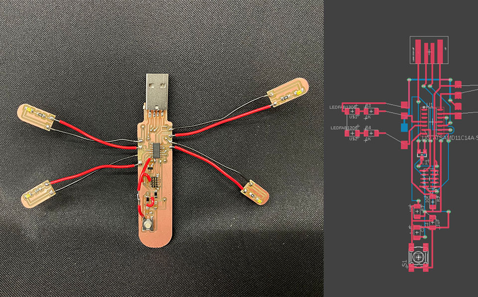
For this week's assignment, my plan was to design a fairly thin / slim pcb board with multiple LED's branching out of the circuit.
Given that I do not have a background in electronics design or related, I began by analyzing exisiting designs from the fab academly website, previous student work and ones available on the courses's website.
I started by using Autodesk Eagle, built in within Fusion 360, since I am attempting to learn how to model in fusion. Attending the recitation by Zach from the CBA shop was a very helpful kick start.
To add a layer of complexity, and perhaps a consequence of making a thin board, I had to deal with flip / 2 sided milling.
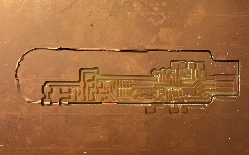
Here you see the first attempt [did not function] both in physical and digital design.
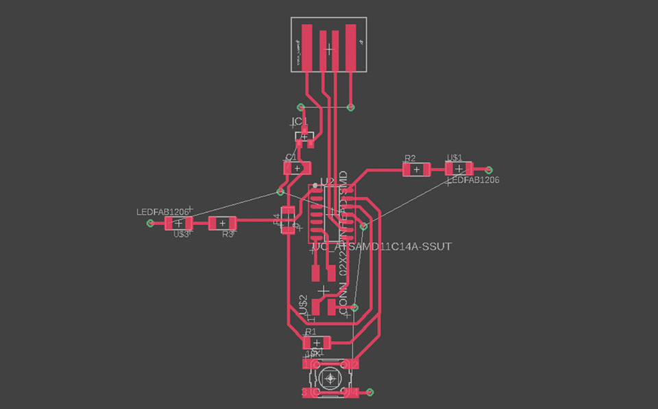
The final design in Eagle using mainly the fab library and 21 vias. The reason for the excessive vias is 1) I thought it is cool and 2) I was trying to avoid using 0 ohmz jumper resistors [I did not like the concept of it].
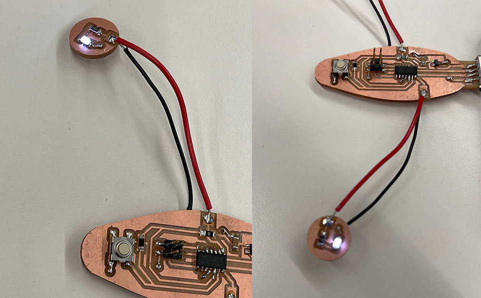
Because the LED and their 1k resistors are detached from the main pcb, I had to do those in a separate file. The initial idea was to connect them through 3D-printed parts using conductive filamnet available at the science center lab.
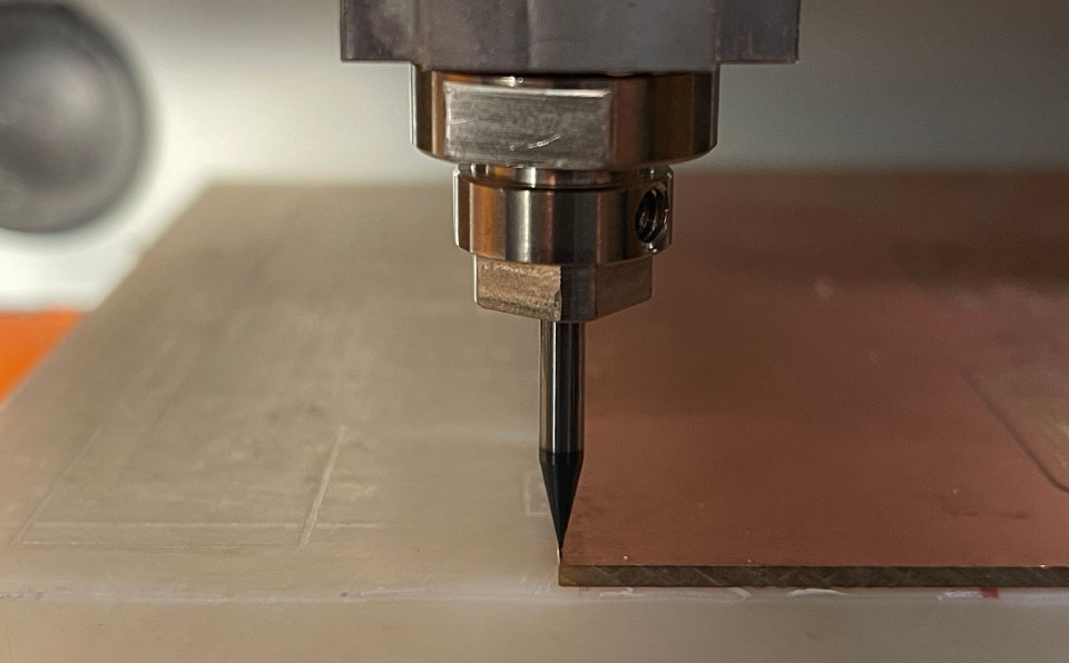
The expoted layer [3] are the top mill, the vias [drilled from the top] and the back side mill. I had to use adobe photoshop to fill in the raw images that were exported from Eagle, clear out the text and invert some [the vias] layers.

Whereas in single layered pcb board, the origin or placement of the stock on the machine bed does not interfere with precision much, when milling both sides, the origin of the machine and the stock is critical to get the two faces to match.
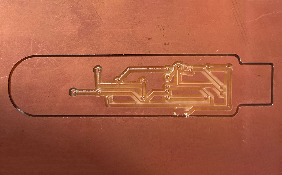
While I did not do that, and hence ended with a failed first attenpt [as you will see shortly], this image is from the second try, where I calibrated very precisly the location of the stock material on the bed, and marked both on the bed with a pencil + kept a record of the xyz location.
... and as mentioned above, this is the failed first attempt. After milling the top, the vias and the bottom, the contour layer showed the awaited disaster: the top and bottom do not align. So I had to spend the next hour attempting to understand why did this happen and how to resolve it.
My conclusion was as follow: 1) the stock was not flipped correctly given that I was using an asymmetrical stock [scraps], 2) the mirror tool in photoshop is problematic and instead I should flip the material not the canvas.
... but, another hour later, the board is milled correctly taken into account the solution above!
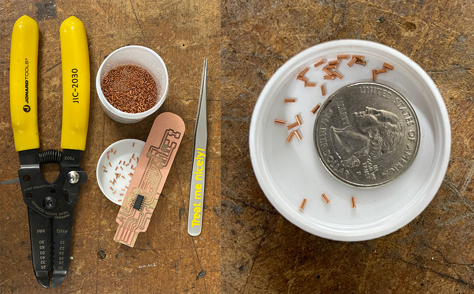
I have not head how to connect vias, so I started looking through the cabinets in SC 102 lab until I discovered the "copper pins", their scale immedietly gave me the clue that those would be inserted in the vias. They are tiny, really tiny, so working with them is not very easy and require patience and a good mood.
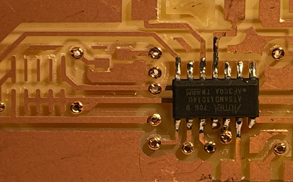
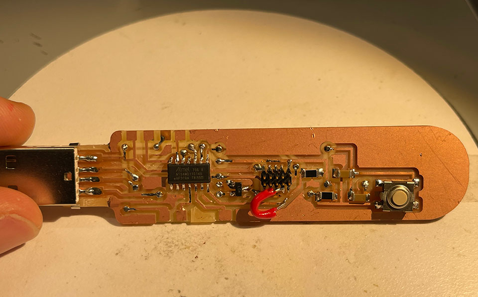
After few minutes they were set in the board and ready to be covered with solder. So the board stuffing process begins now.
Everything seemed fine, until I noticed that I have missed one key connection, the reset link in the SAMD11C14A microprocessor. I added a small jumper wire, which was somewhat a hassle to do given how close the pins are to one another and how small it was.
Testing did not go as planned, I tried several options, but the board was not detected with openocd. I figured that the problem was due to bad design not bad milling. The voltage abd current tests were successful. But because I was referencing multiple designs, I had some wrong assumptions and doubling of components [resistors and capacitors].
It was very difficult to edit now, and instead I decided to mill and stuff another one. This time I thought I had to fully understand the concept before doing any execution.
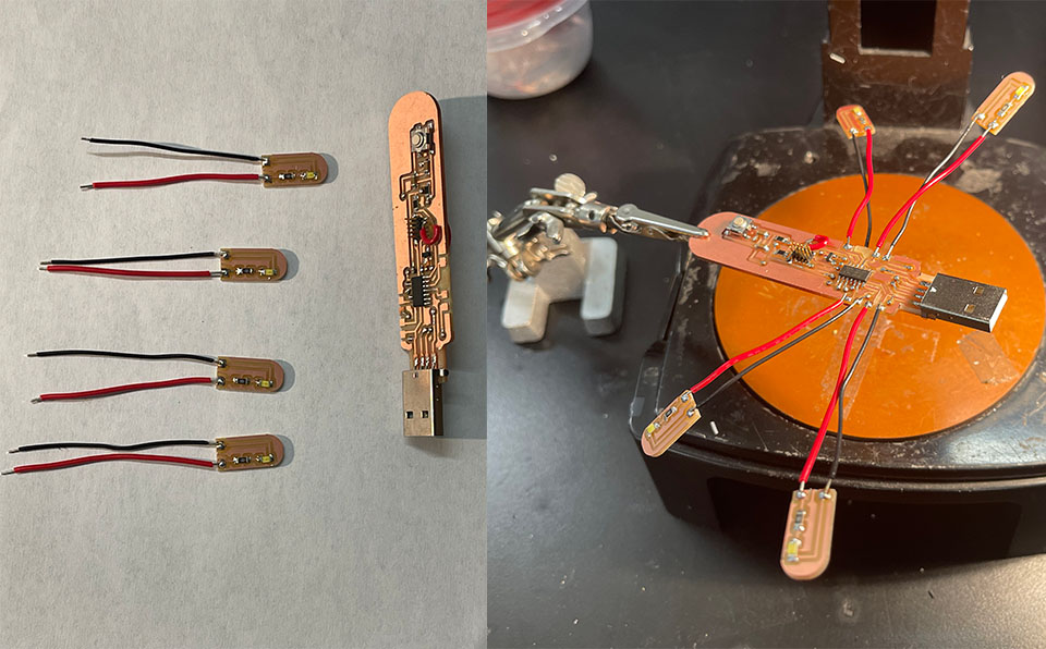
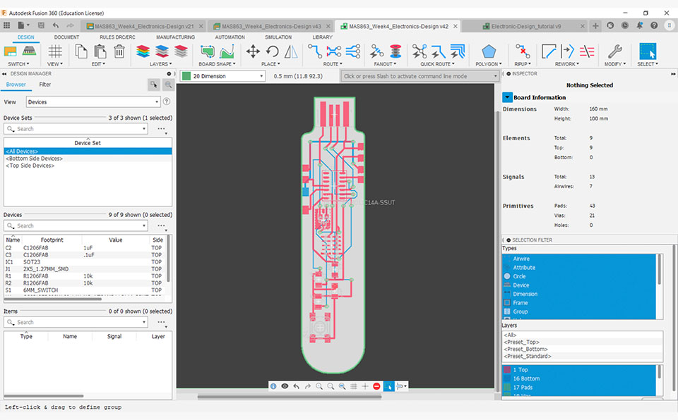
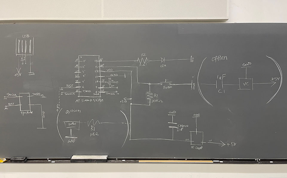
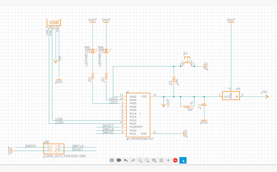
The board is my best friend. A place I can sketch, clear, sketch and layer freely and at scale. I started by centralizing the SAMD11C14A mp, understanding its pins from the digi-key library spec sheet. I think connected the other required components. Colleagues started walking in and through questions and discussions, I started understanding what components connect to what and where.
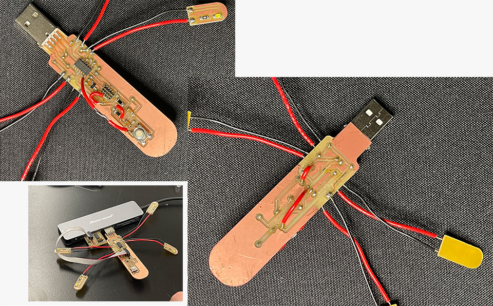
Updated design, this time alittle wider and the bottom is ground with 6 vias.
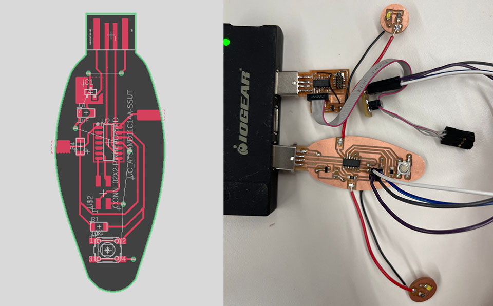
The board blinked using edbg and arduino example file.