
The assignment this week was to mill, stuff and test a PCB. I was freaked about the soldering part, but also ended up running into plenty of issues with the milling, which frankly I assumed would be easy.
I used the Roland SRM-20, and had a ton of trouble getting the 1/64” bit to cut through the copper for the traces.
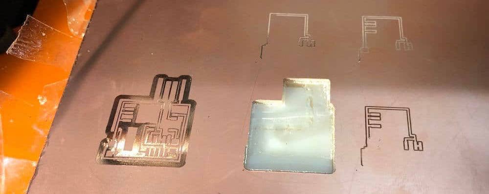
On Nathan’s suggestion I bumped up the cut depth a little bit, which worked but left me with board that was pretty ugly/burled board.
I saw that Gabby was able to cut some clean boards on the same machine I was using. So I took a crack at it again and finally had a slightly better result. One change was I started really pulling the bit down while tightening the screw at the very end.
After some exacto-knife clean up, here’s where I was at. The bottom corner of my last version came out solid, I don't know why the rest got more burled. But good enough (maybe)!
I stuffed my board on Sunday, and I have to admit – I enjoyed soldering more than I thought it would! I mean it was really frustrating. But it was sort of zen and intensely satisfying when you get a smooth joint.
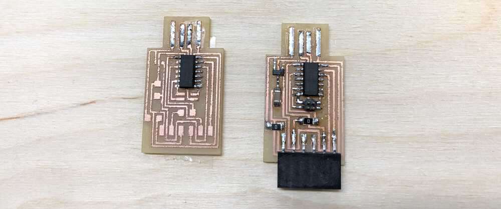
I started with my crappier board and it’s a good thing I did. Because I put on the D11C first and didn’t realize that it had an orientation, so it was backwards. Got everything on in my second attempt, but had a lot of trouble with the tiny O resistor on the left edge.
In general the most difficult part for me was initially placing those really tiny pieces. I had to get a pretty big spot of solder under a corner to get them to stick, and then they’d end up a little lopsided. I also was a slow solderer, so I ended up with some melty plastic.
Alas, I went in Monday morning to get my board tested, and it wouldn’t boot. Nathan and Kevin both inspected it and there wasn’t anything obviously wrong, and power seemed to be moving through it ok. So I guess one of my components wasn’t working, either because I was unlucky or (more likely) because I melted it. Or my burls were causing the traces to cross somewhere I couldn’t see. So I decided to just go ahead and try to make a new PCB, a blink board this time.
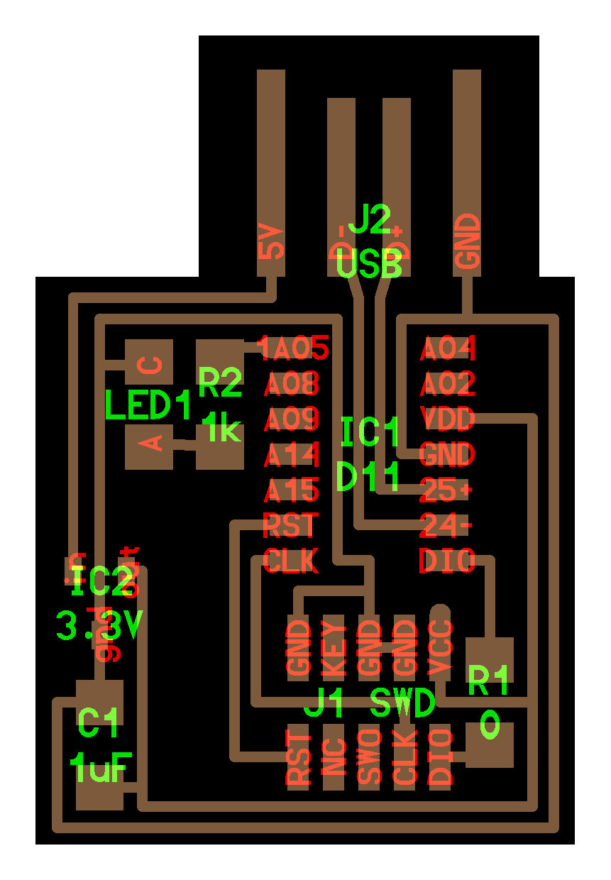
The good news is that I was finally able to get two really clean cuts on the mill. I really pressed down on the board to get it too adhere, and also bumped up the cut depth by 25% after I started with yet another ”not all the way through” trace failure. Here’s my blink boards after exacto-ing, with one of them stuffed.
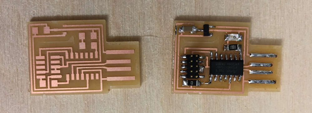
On Tuesday morning, I brought this board in for testing and it booted! Glorious day. We were able to load the blink program on and then ... nothing. No blinking light. On testing it seemed like the a pulsing electrical current was passing through the LED, so the only thing left to try was replacing the LED.
On Wednesday morning, I made this switch and realized my horrible, horrible mistake. The blink board diagram called for an “LED1” so when I was stuffing my board I’d grabbed from the tray labeled “LED 1R,” which I figured was a red LED1. I decided to investigate a little better for this final swap.
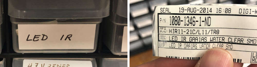
“1R” was actually “IR”! It was an infrared LED the whole time. So my board had probably been working fine, it was just blinking outside the visual spectrum. I removed my LED (which was hard, could use tips on that) and swapped on an LED G. And sure enough.
Victory. And it only took all week!
Meanwhile, my groupmates did an excellent write-up of our team milling assingment. Our mill could handle ridges down to 0.01” (wow), but it wouldn‘t trace channels below 0.016”. I contributed slightly by starting a team directory that we’ll use for future assignments.