week 3: electronics production
Prior Experience: 1/5
For some reason, I was really confused this week. I used a PCB that they provided (which basically just had a button and an LED) for a class last year, but I had no idea what it meant for some reason. However, I've soldered before minimally, when I was a child and in that class. In hindsight, I don't know why I was so confused about what a PCB was, or what the point of this week was, but I think I just didn't understand why/how it connected to microcontrollers, or what a microcontroller was, even though I had programmed an Arduino to make an LED blink before. I basically just did not understand what was going on at all. I think one issue was that my main exposure to circuits was in E&M or from a physics/Maxwell's equations point of view, so I was really confused about how circuits were useful or could do anything. I probably would have been a lot less confused if you asked me about Gauss' Law or something.
This is where I'm starting out:

A PCB is printed circuit board, where the circuit is formed by thin "traces" of copper that conduct electricity, rather than a bunch of wires.
Here's a helpful tutorial on microcontrollers: https://mtm.cba.mit.edu/2021/2021-10_microcontroller-primer/
Step 1: Milling The Board
The milling machine fabricates a PCB based on a given circuit design by cutting into a plate with a thin top layer of copper and a center made of nonconducting material. The milling machine removes all the parts of the traces that aren't part of the circuit, leaving behind only the conducting material necessary to form a circuit. This is a PCB.
I am following the archshop tutorial for the milling machine: https://archshops.mit.edu/modela.php.
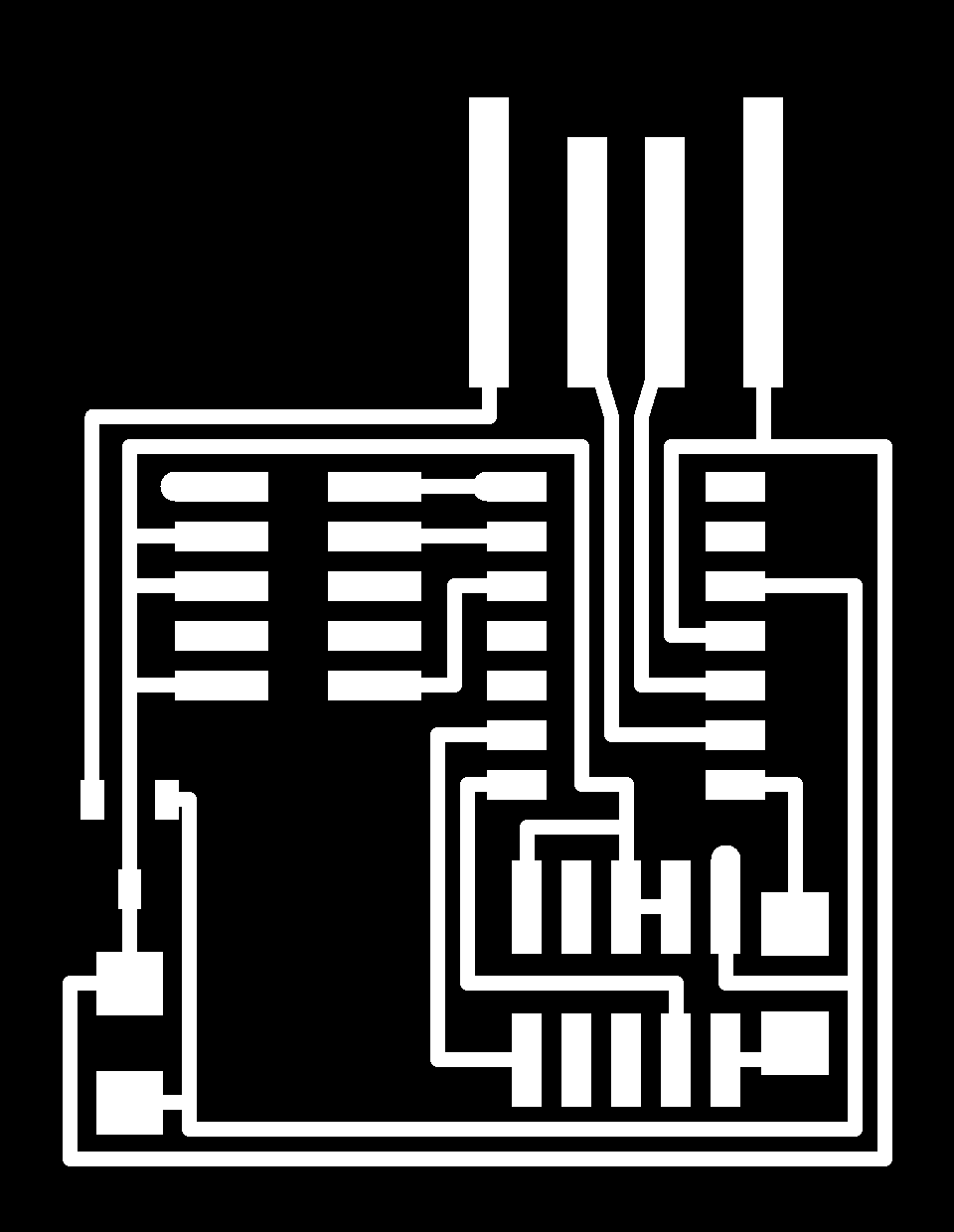
For this week, we were provided a file for the traces (http://academy.cba.mit.edu/classes/embedded_programming/SWD/hello.CMSIS-DAP.10.D11C.traces.png), so that we could focus on learning how to use the milling machine, solder, test the board, and so on.
I used their mods (using the mods.cba.mit.edu) to send the traces to the milling machine. To navigate to the appropriate mod, right click, then click on programs, then open server program, then scroll down to and click on Roland Mill SRM-20 PCB png. Upon uploading the appropriate PNG, the mods calculate what to send to the milling machine.

Cut the Traces
We cut the traces on machine with the 1/64" bit. First, switch the end mill bit to 1/64" by using the Allen wrench to screw it in. Then, set the origin coordinates (x, y, z) to the bottom left corner of where the machine should start cutting. (I used origin: (x = 28, y = 112, z = 0).
Then, to place the bit precisely on top of the plate, unscrew the bit a little and gently use your hand to place the bit touching the board, and then screw the bit back, tightly.
To send the PNG file to the machine, click mill traces (1/64), then calculate, and hit open socket. Next, click send file to device to start milling and hope for the best.

After the machine has finished, vacuum the dust to see if the traces are okay.
"Your traces look perfect!" - my TA, Demircan
Cut the Outline
Next, cut through the board outline with the 1/32" end mill so that the PCB can actually be taken out of the rest of the board material. First, switch the end mill bit to 1/32". Set the same origin as for the traces (x = 28, y = 112, z = 0) and touch the bit to the copper board again.
Now click mill outline (1/32), hit calculate, connect the socket, and send the file to the machine. Vacuum again and use a spatula to gently take out the PCB!

Wash it With Special Soap
Now, you need to wash it with a specific brand of soap and dry it. (My TA does not know what is special about the soap but this is what is used.) This removes random particles on the PCB. After that, dry it off and make sure you don't touch the copper or it might rust.
Solder Random Electronic Components Onto the Board
Next, once the copper traces have been cut out onto the PCB, you need to solder a bunch of random electronic components onto the board to actually let it do anything.
Finding The Parts
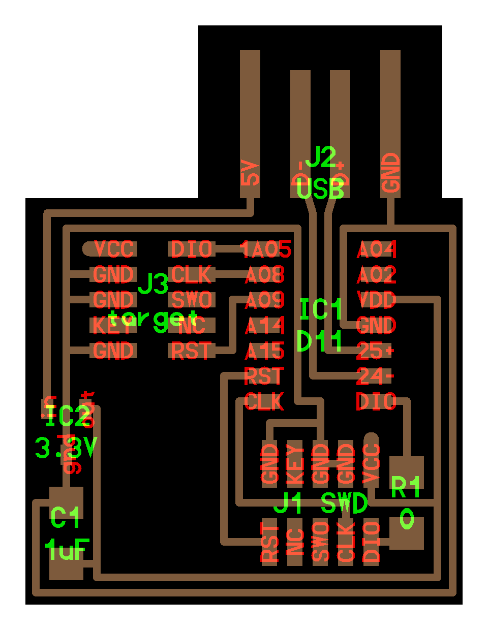
For this week, we were provided a diagram to follow for the electronic components: http://academy.cba.mit.edu/classes/embedded_programming/SWD/hello.CMSIS-DAP.10.D11C.png
I got a piece of cardboard with double sided tape on it to stick my parts on.
Now, I look for the parts in the bins.
- IC1, D11: This is the most important part, the microcontroller.
- J2, USB: This is built in to the PCB (where it sticks out).
- J1, SWD and J3, target: These are the connectors/connection headers. It allows you to connect things to your board.
- IC2, 3.3V: This is the voltage regulator. It makes sure you don't go above 3.3V.
- R1, 0: This is a zero Ohm resistor.
- C1, 1uF: This is a 1uF capacitor.
All the parts are quite small so the tape keeps them from flying away.

Soldering
I adjust the lights/magnifying glass to look at the parts so that I can actually see what I'm soldering.
Note that the circle on the D11C microcontroller always corresponds to the corner on the PCB where there is a slightly rounded edge; orientation matters.
To solder, turn on the iron and stick the tip on the copper on the PCB for a bit to heat it up, and then add the solder. Then, add the corresponding electronic component. Each of the rest of the legs can be soldered on as usual.
I soldered according to the diagram. It took a long time.
Here's the finished product:

Test the Board
Finally, I tested the board.
Jen helped me to test my connections with a multimeter to make sure there weren't any issues with my soldering, and to cut off the excess copper for the USB port connection.


Jen and I spent a while debugging the board, and then we tried programming it using the archshop computers with edbg.
Group Project: Characterize The Machine
We cut some lines as a group to characterize how thin of a line the milling machine can cut.
 (Thanks to Lakshmi for milling this!)
We were provided the files for the traces (http://academy.cba.mit.edu/classes/electronics_production/linetest.png) and the outline (http://academy.cba.mit.edu/classes/electronics_production/linetest.interior.png).