Board Design
I wanted to design an ATSAMD11C echo board using the 10 pin header (you can view the starting png here) with one extra button and LED. Using EAGLE on Fusion360, I added the following components (almost all under the given fab library) to my schematic:
- Microcontroller - UC_ATSAMD11C14A-SSUT
- Header - CONN_05X2_ARM_DEBUGTDC2050-IDC
- Voltage Regulator - VR_REGULATOR-SOT23SOT23
- USB - CONN_USB-A-LC
- Capacitor - CAP_UNPOLARIZED2220
- Button - SW_SWITCH_TACTILE_6MM6MM_SWITCH
- LED - LED5MM
- Four resistors - R1206FAB (one is 1000 ohms for the LED, and three are jumper resistors)
- A bunch of grounds - GND-BAR (there are no GNDs in fab, so I used the ones in Power_Symbols/Tutorial - Fusion360
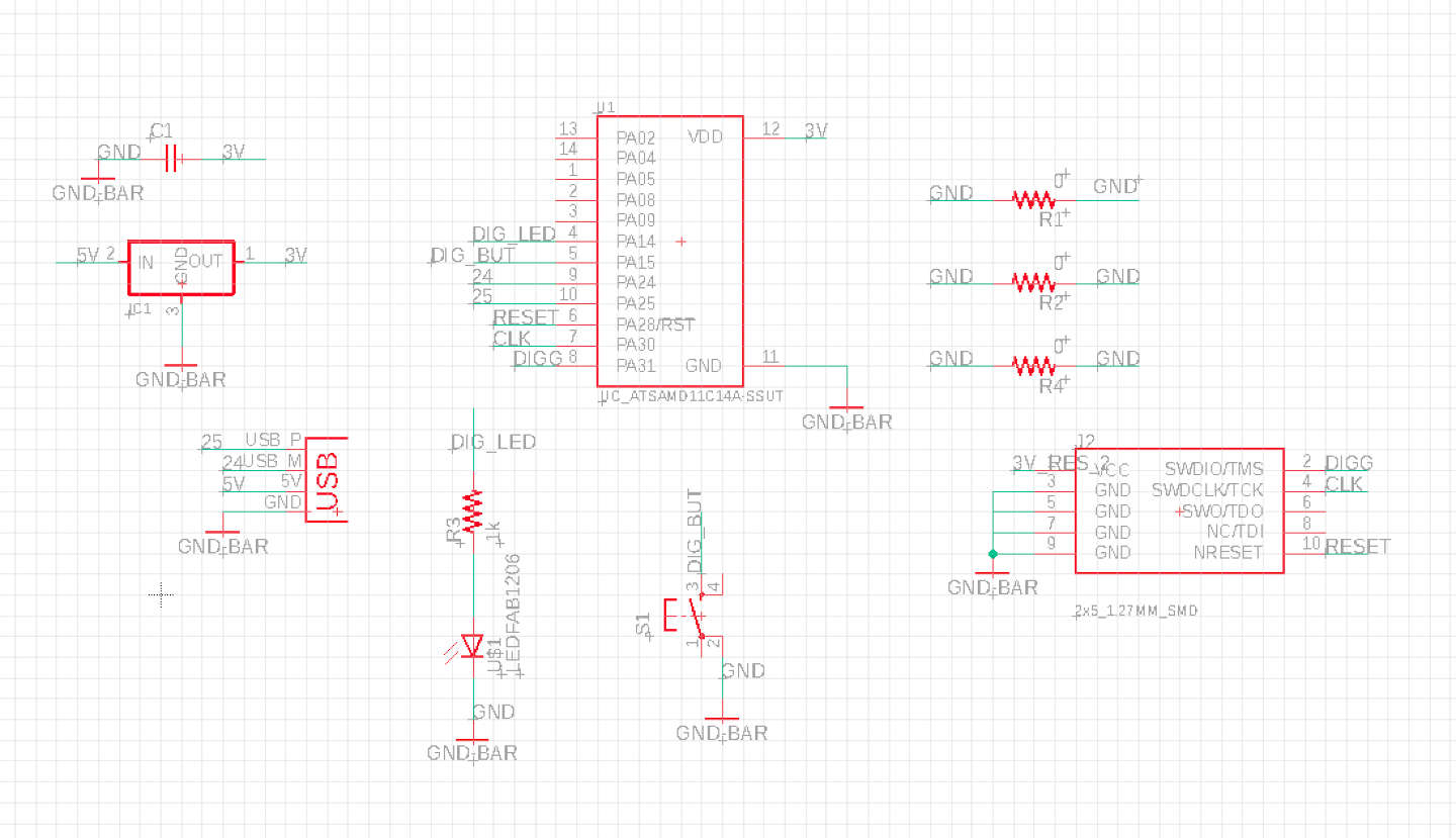
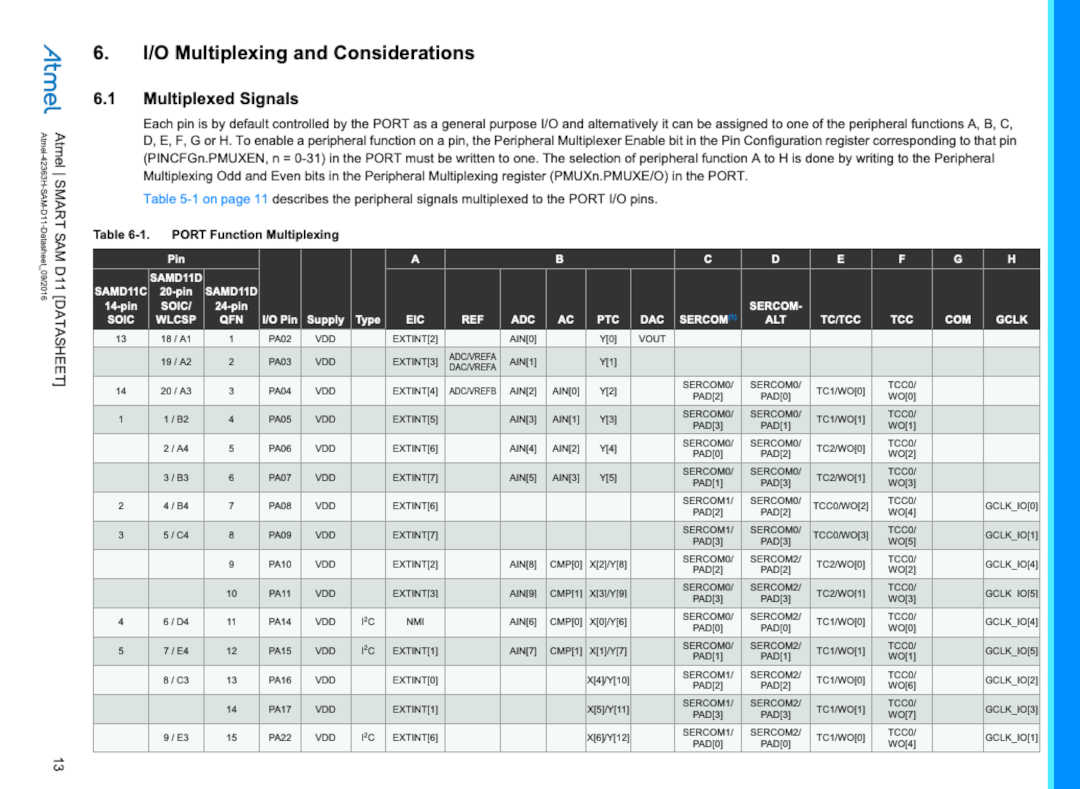
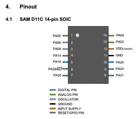
In order to make the connections (the green "wires"), I used the microcontroller datasheet to know which pin numbers corresponded to what functions. More specifically, the PORT Function Multiplexing table shows the mapping between the 14-pin pins and the header (under the COM column). In order to figure out which pins the LED and button go into, I found the digital pins schematic in the datasheet.
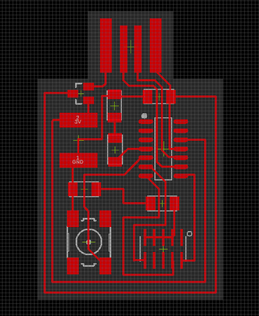
Afterwards, I turned the schematic into an actual board design! It took a lot of pointing and clicking to play around with the wires to see how I could space things and make it work.
Board Creation
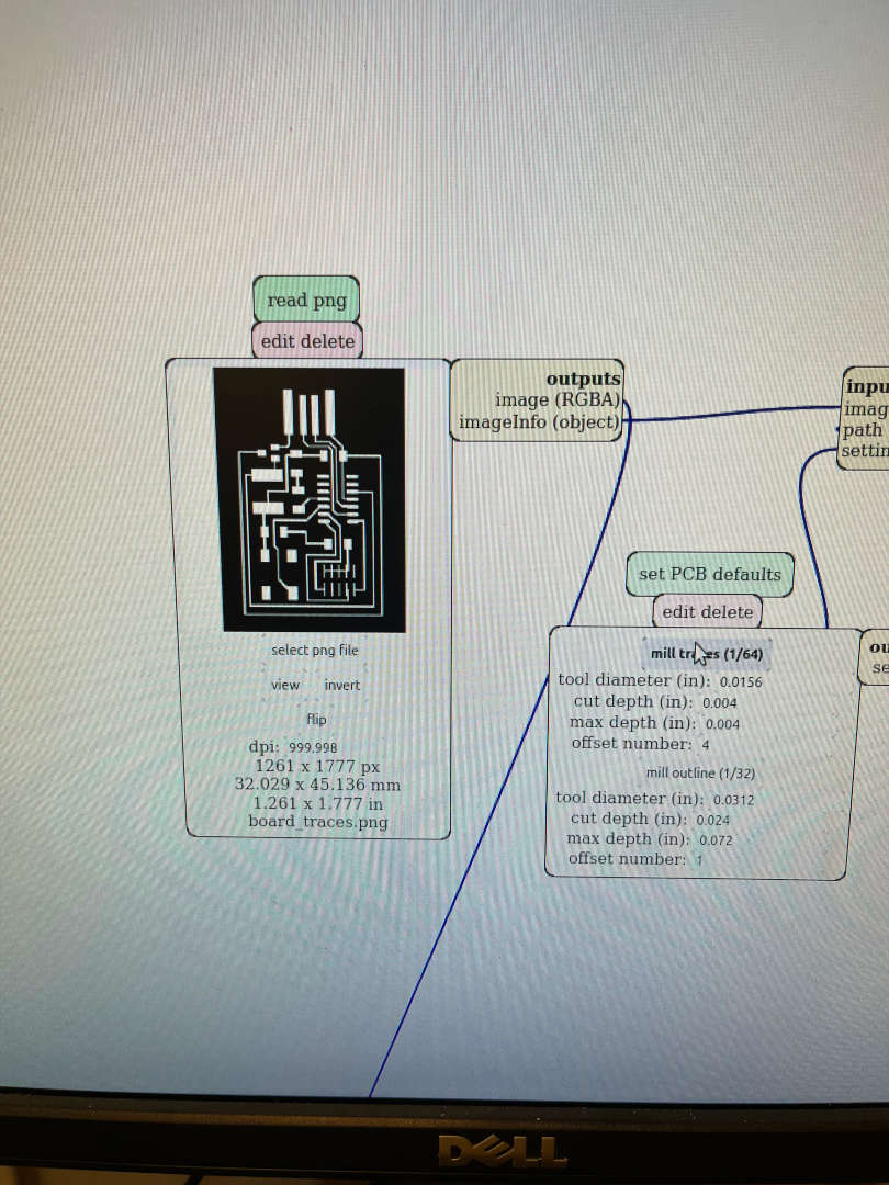
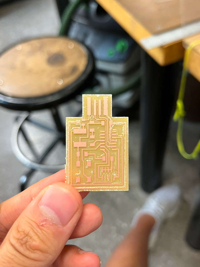
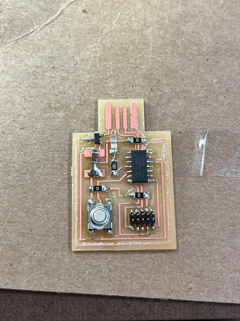
I exported the design (both the traces and the outline) into Photoshop, where I cropped the image. I had to be careful to make sure that the crop was the same area for both the traces and the outline. If not, then the alignment would be off and the two mills would overlap. I solved the problem by watching the pixel locations of the top left corner and bottom right corner for the crop. Afterwards, I milled the PCB board, found the physical parts, and then soldered it on!