Week 3: Electronics Production
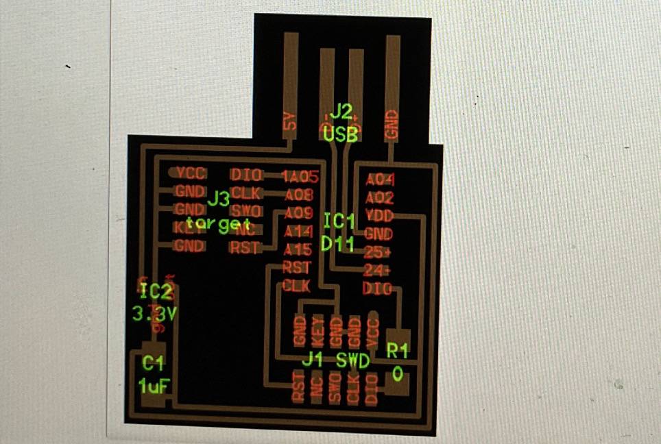
This week's project was to create an in-circuit programmer, with a microcontroller, by milling and stuffing a pcb. The image below is the schematic for the PCB I was trying to make.
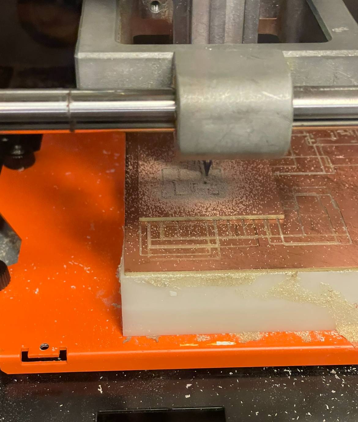
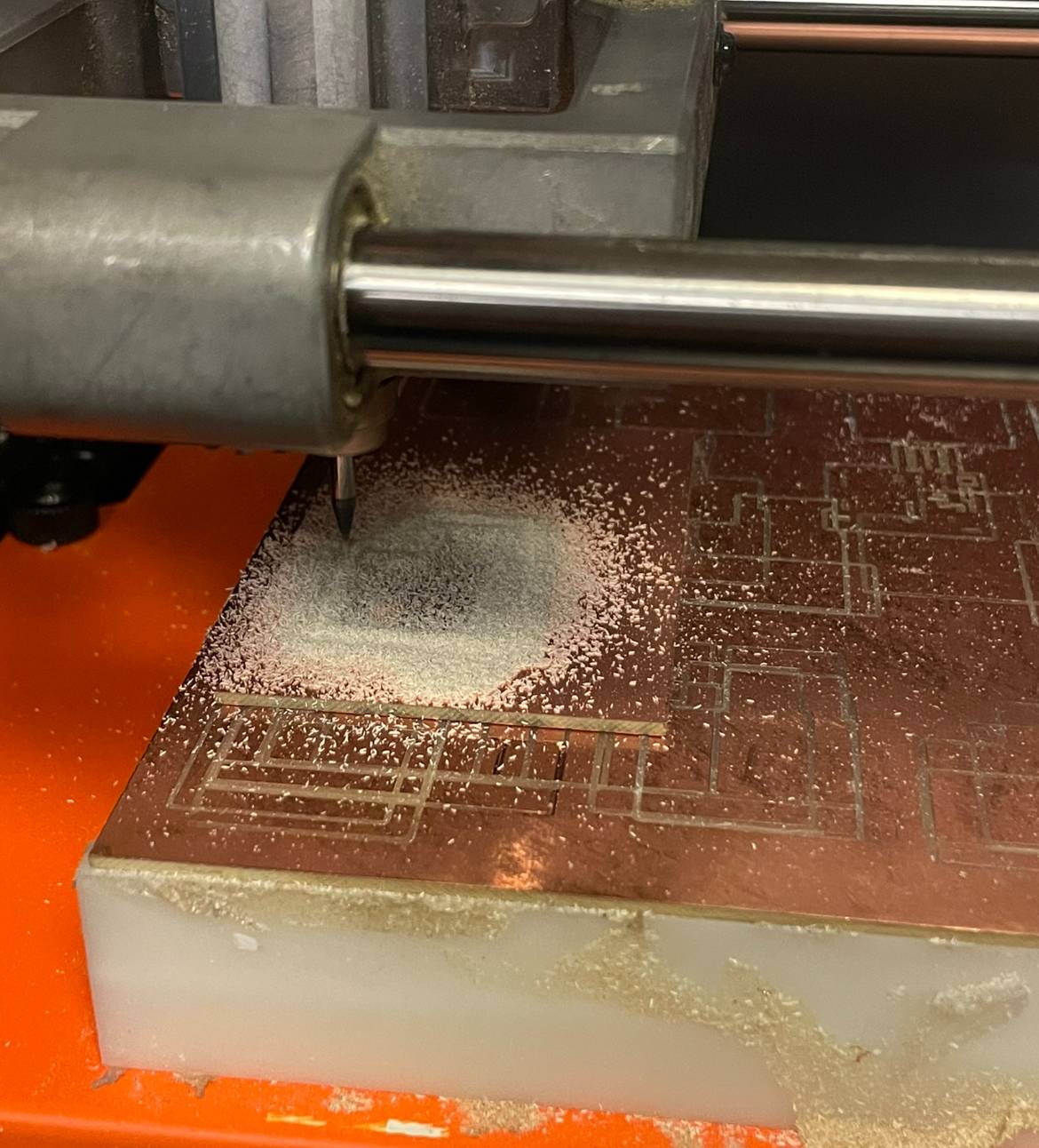
The first task was milling the PCB. This took a couple of tries, as on my first attempt I meant to do the outline but put the setting for the traces instead, so the copper wasn't cut all the way through.
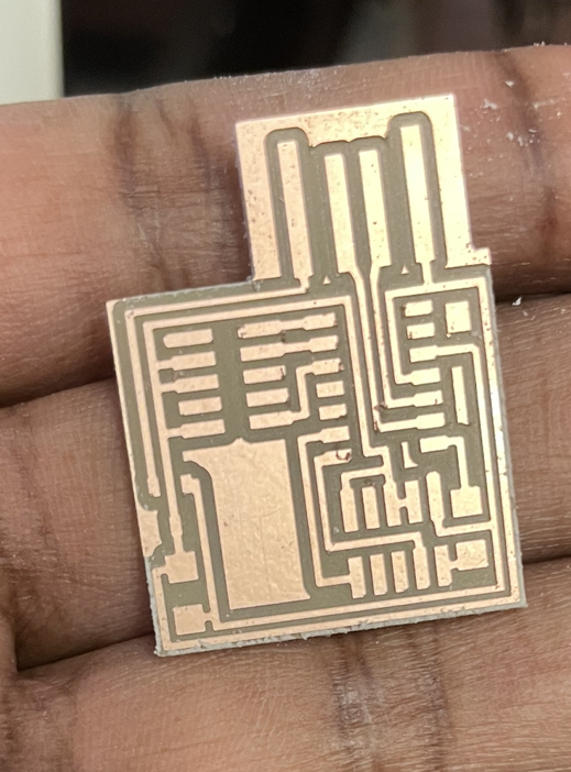
However, my second attempt went a lot better:
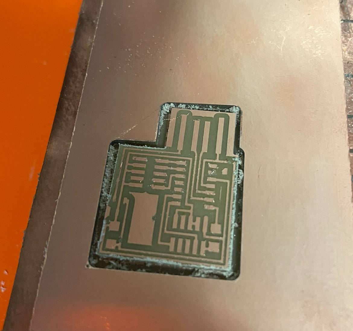
And here's what the final pcb looked like:

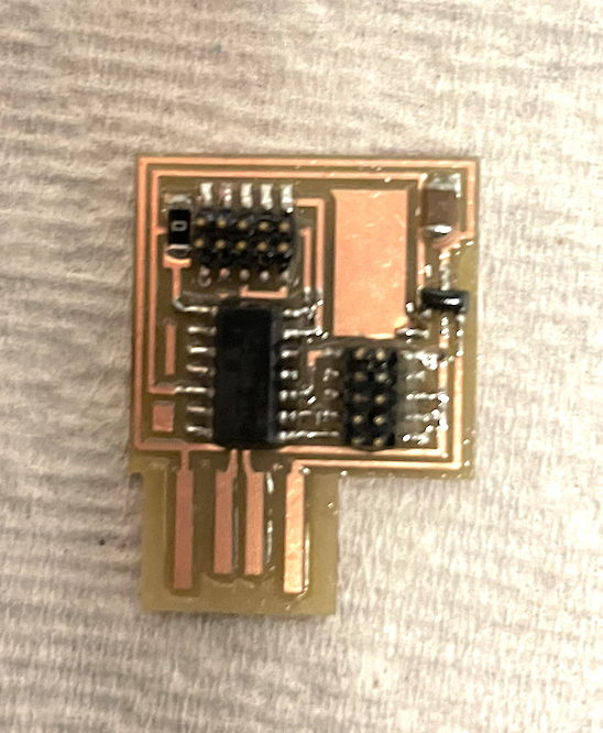
Next was stuffing the board and soldering the components on. This process was more difficult, since I wasn't used to soldering such small devices. There was a lot of flux and solder wick used to ensure all the components were in place, oriented correctly, and ensure the soldering was neat and clean. This was probably the most time-intensive component of the project for this week; pictured below is my stuffed PCB:

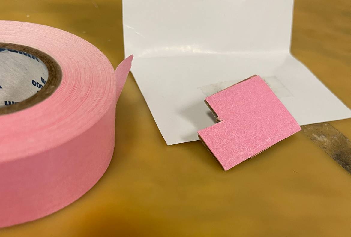
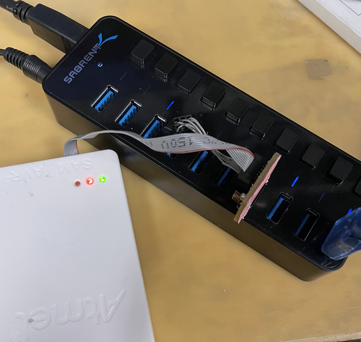
Last was testing and programming the board. In order to make the usb part of the chip thick enough to go into the usb port, I put a few layers of tape on the back
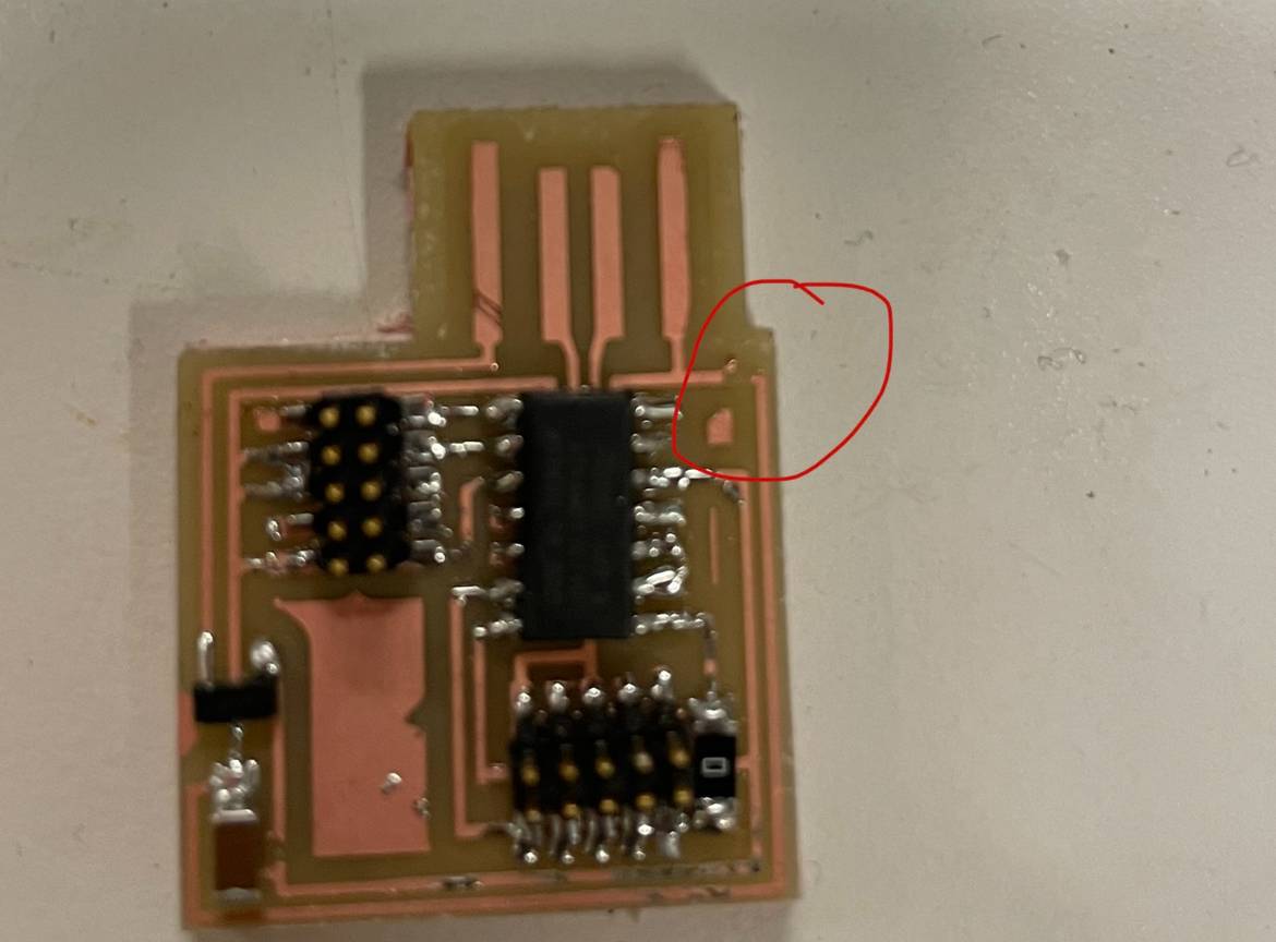
However, in the process of testing and debugging, an issue was discovered. The ground traces weren't fully connected, since the trace was broken; I did some more soldering to reform the connection, though found even more incomplete connections

*Note, in this picture, the plug connected to the header on the PCB was oriented backwards, but I switched it shortly after taking this picture.
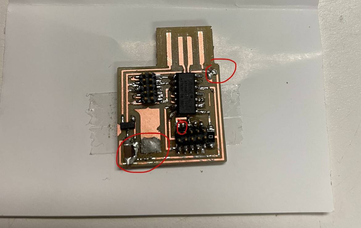
This was my finished attempt at fixing all the connection issues, featuring an unintentional giant glob of solder near the capaciter; although, when I used the multimeter, it didn't seem to affect the ground connections, so despite not being the most aesthetically pleasing, it didn't apparently seem to make a difference while debugging or have a negative effect on the connectedness of the components?
Alas, this still did not provide a working result. When redoing this process, I would remill the PCB upon seeing the traces initially--given that the expected result would not have resulted in such variable traces--to avoid having to reconnect/resolder broken traces, and to provide myself with a bit more surface area and a better base for good contact between my components and the copper underneath. I also think my solderinng could have been cleaner, so I would attempt to fix that by applying less solder and utilizing the flux more to avoid having solder connecting components or traces that shouldn't have been connected.
On my second attempt to create a functional PCB, the traces came out a lot cleaner, and the solder seemed to be a lot cleaner than before--I did end up having to re-solder the microcontroller since I had initially put it on in the incorrect orientation (with the small dot in the bottom right corner instead of the top left corner), but aside from that, the soldering seemed to go a lot better than before.
And even more exciting: this PCB actually worked! With the knowledge gained from my past PCB, this one was improved drastically