Week 7: Embedded Programming
This week's project was to browse through our microcontroller's data sheet, and use our programmmer to program the board to do something.
I decided to make a board using the SAMD11C, given that I had worked with it before, though I wish I had tried using other microcontrollers to get a sense of which ones I preferred most
The first part of creating the board was looking through the data sheet for the D11C in order to be able to create a schematic with the components I wanted (mainly, a button and an led, along with the other required components for being able to implement the actual logic)
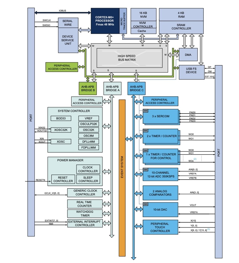
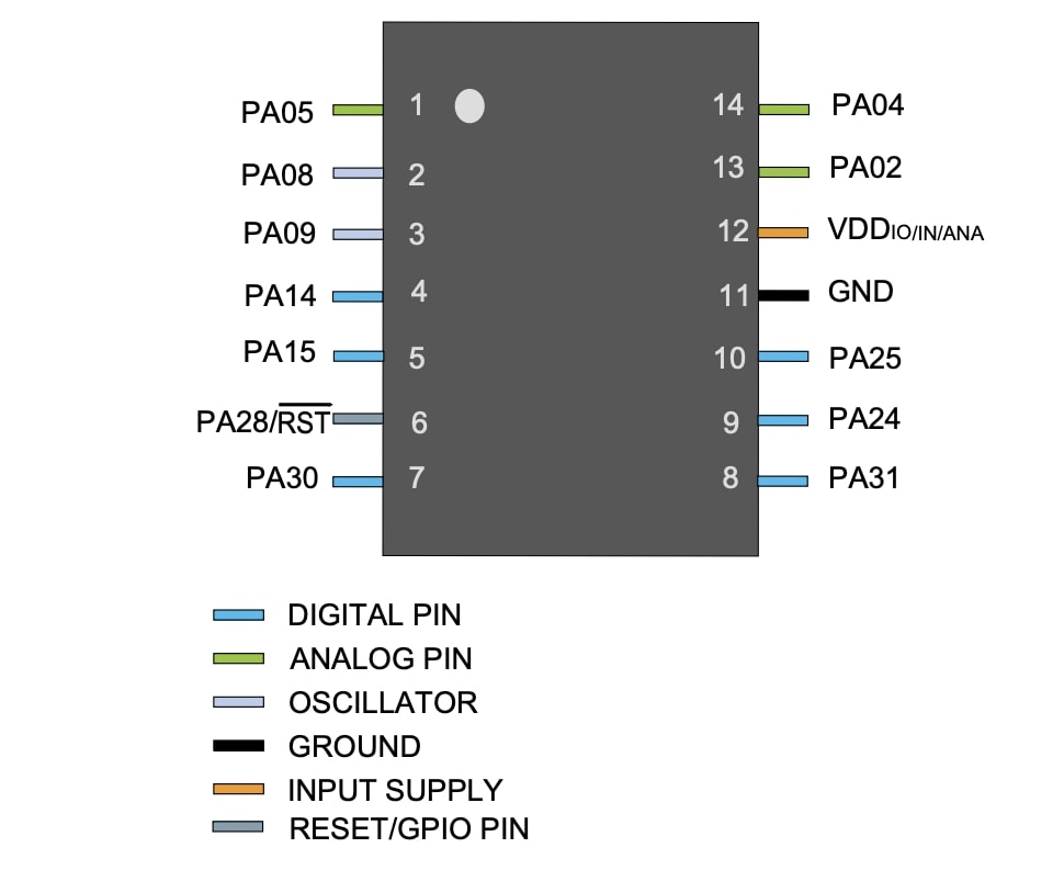
(d11c info diagrams)
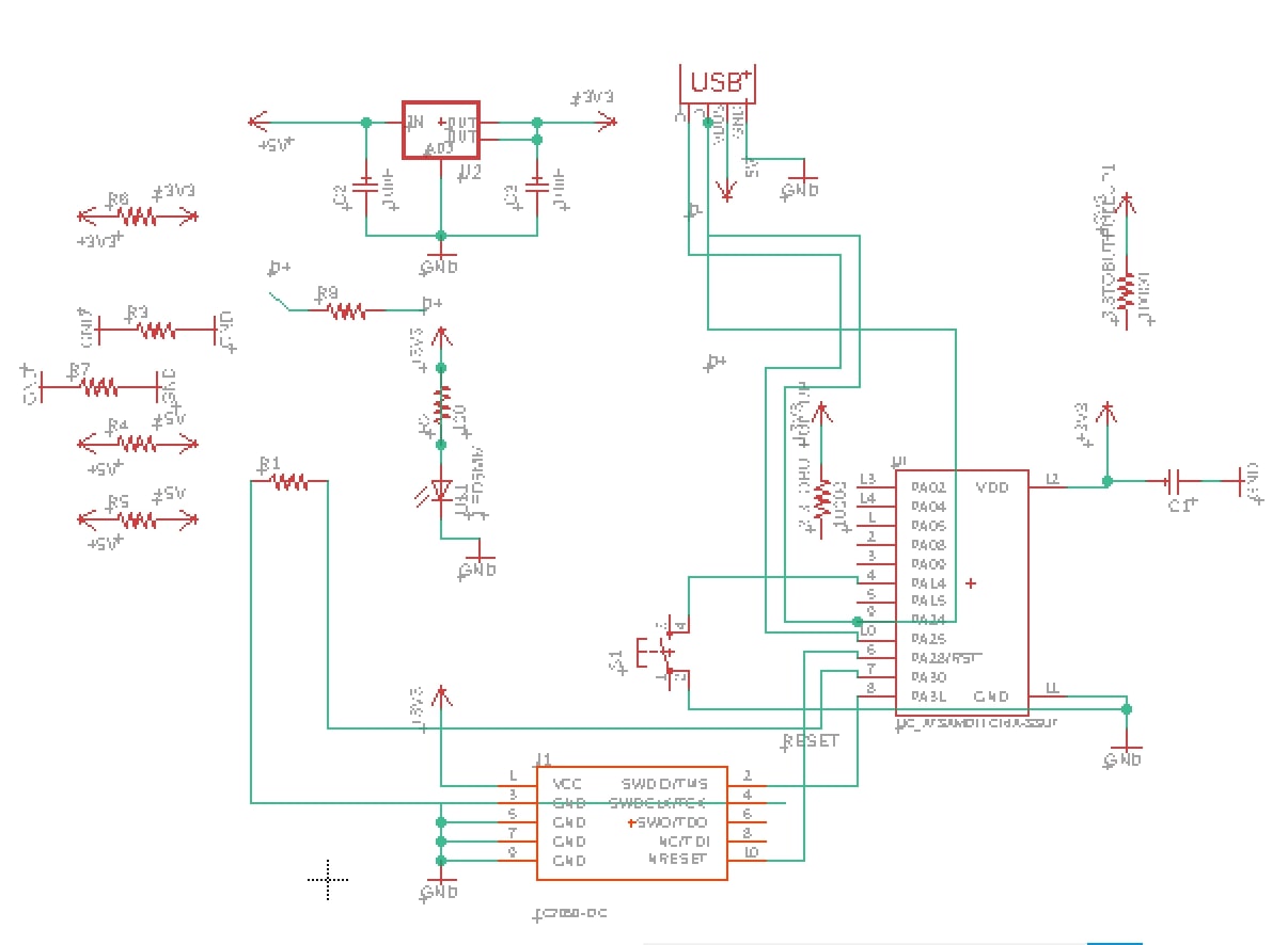
Once I had looked through the data sheet for the information I needed, I began creating a schematic in Eagle, using the pcb design methods we had learned before.
This was my finished schematic:
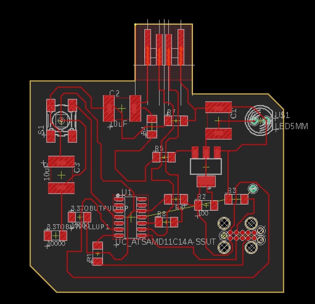
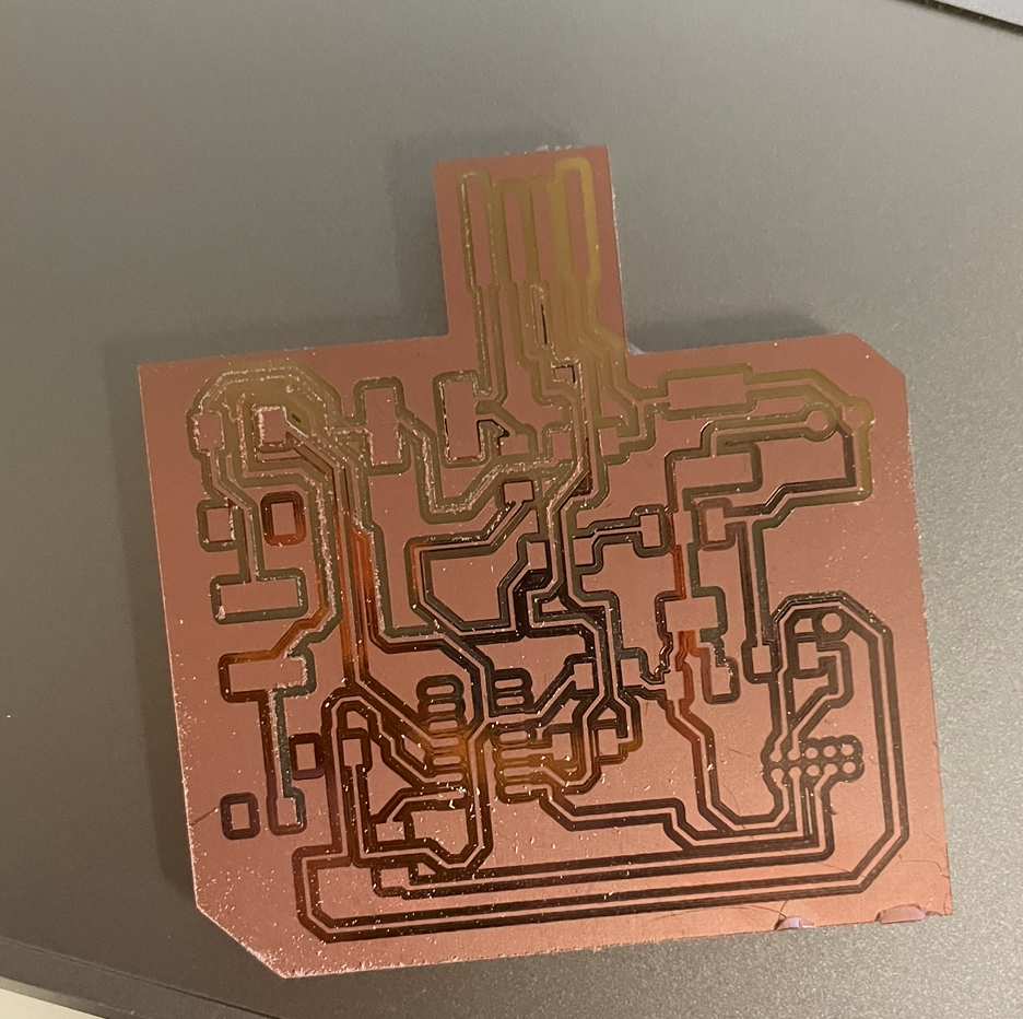
With the schematic done, now it was time for place and route--I ended up having to use a lot more jumpers than I would have liked to, and I think if I were to redo this process I would try to organize my board better, along with potentially using a different microcontroller. Before finalizing my PCB design, I made sure to do a design rule check, and then exported the images of the traces and background to be milled.
(pcb finished and traces)

(pcb finished and traces)
During this process, I also wanted to get more acquanted with C and the process of programming the boards, so I examined Niel's echo and blink code to get a sense of what the programming code generally looked like. I also referenced Julia Elbert's (from the HTMAA 2017 Harvard section) documentation and code for this process as well. Also, I used the Arduino IDE for this part of the process.


The image on the left is an example of the Arduino IDE upon initialization, the second sreenshot shows what the main method for actually executing the code/loop, after all of the setup has been done. This code is the example of the blink code, and what I intended to build upon to execute a more complicated loop.
I then went on to mill and stuff the board, and planned to use the simpler working code above to test its functionality after stuffing it. This would begin the trial and error portion of the project.
`
This is an image of what the milled pcb actually looked like, along with all of the components (and the strip the length of the 0 ohm resisters I would need, carrying them this way was simply easier). I wanted to avoid having to restuff or remill a board at all costs, but with the start of this process, the process of debugging also commenced, and I wanted to make sure I'd be able to display and better remember which parts I would need (though was also aided by the schematic I had already created)
.jpg)