Week 3: Electronics Production
Assignment
Assignment Details
👯 group assignment:
- characterize the design rules for your in-house PCB production process
- extra credit: send a PCB out to a board house
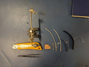
PCB Milling Process
- Clean the inside milling machine and milling platform as necessary
- Place double-sided adhesive to a clean copper plate
- Smooth the tape onto the milling platform until plate is maximally flat against the platform
- Grab the necessary end mill
- Make sure milling machine is powered on
- Open mods
- Gently load the end mill into the milling head until desired depth is reached
- Align milling machine head to home/origin in mods
- Adjust machine settings via mods until the end mill is barely touching the surface of the copper plate
- Start milling process in mod
- Repeat steps 10-12 as necessary
PCB Design Rules for Manufacturing
- Measurements should be in Metric units
- Set solder mask clearance between 0.0508 mm and 0.1016 mm
- Do not allow blind/buried vias
- Do not allow micro vias
- Keep the shortest path between components
- Group related components with test points for probing
🐇 individual assignment:
- make an in-circuit programmer that includes a microcontroller
- mill and stuff the board
- test it to verify that it works
- extra credit: try other PCB processes
🐇
So, I've never milled a pcb before. There was a lot of trial and error obv. I need to get the bit size, trace depth, and position of the substrate
Then there was the removing the copper, which I had never done.
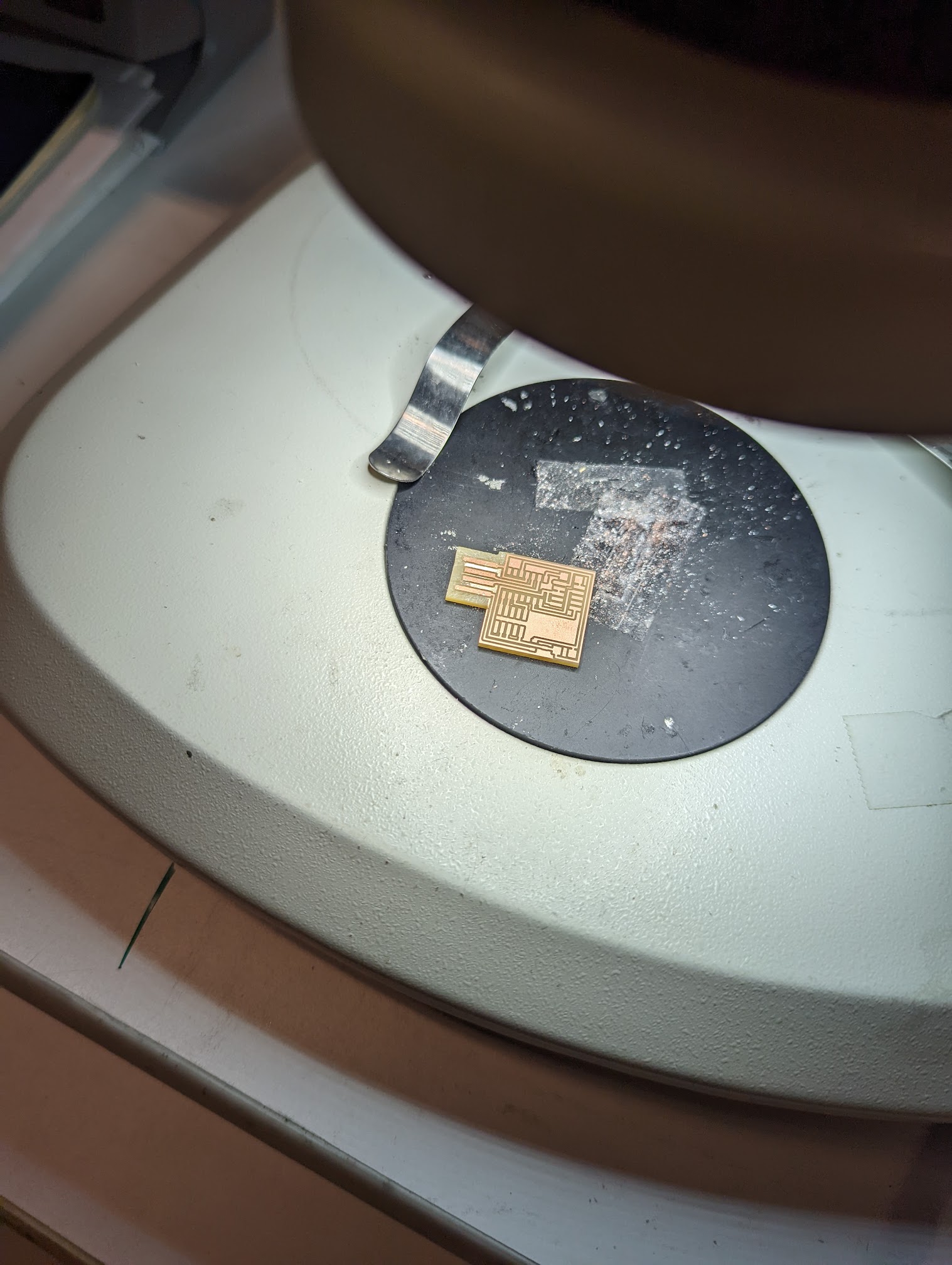
I still have yet to solder the componens, but a hack that another student showed was that one doesn't need to peel all the copper of the substrate
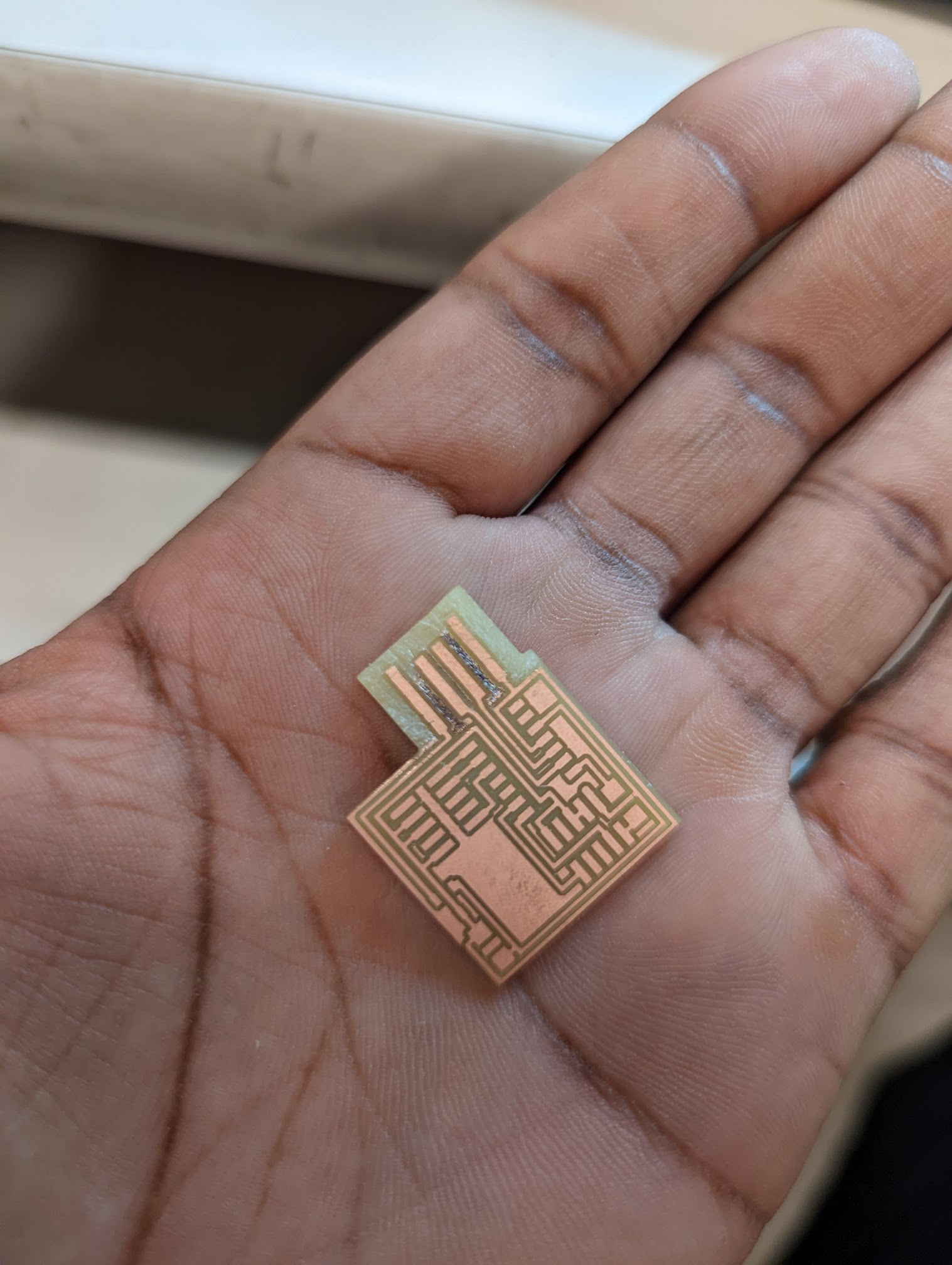
Anyways, I have all my tools to start picking and placing the components on the board.