INTRODUCTION

This week was on gaining skills for milling and stuffing a pre-designed PCB as well as programming it. The assignments were two-fold; a group assignment where we characterize the design rules for in-house PCB production to define the minimum feature size, and the individual assignment where we trace and cut a pre-designed pcb using MODS, stuffing with components, uploading the programmer and finally to verify that it works.
GROUP PROJECT
1.1 Characterize the Design Rules: Roland SRM-20
This week’s group assignment was to characterize the design rules with three-axis Roland SRM-20 mill. This was necessary in order to calculate feature size; that is what the minimum width for both the traces as well as the gaps between traces in the PCB design should be.
1.2 Materials and End Mills
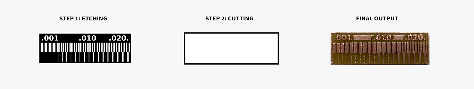
Step 1: Etching
Together with Miana, Wedyan and Lauren, we worked on a single-side copper coated plate (with the sacrificial layer) of 15x8cm. The first step was to attach the plate to a flat and clean cutting bed using double sided tape. For ease of removal, we used the thicker double-sided tape in multiple sections of the board, every other 5mm, to keep it stable on the bed. Next step was to fit the 1/64" end mill loosely to the head prior to setting the origin for etching. Using MODS interface, we set the origin to the part of the plate which would reduce the amount of waste material, but also provide us enough distance to etch and cut later. The Z axis was set at 8 mm, afterwhich we dropped the end mill to touch the copper plate and jammed it in place using the allen key. Once this step was complete, we uploaded the line test traces .png file for etching the conductive traces and let the machine do its magic. Once etching was complete, we vacuumed the dust and particles.
Step 2: Cutting
For this step, the plate should be kept in place while changing the end mill to the 1/32" thick one. Once the end mill is changed, a similar process of recalibrating the origin is conducted. Then, line test interior .png file for the cut file is uploaded and the PCB is cut according to the design. Once the cut process is complete, the fairly larger particles and dust are vacuumed once again before taking the plate off the machine bed.
1.3 Minimum Working Trace and Gap Width
We found that the minimum working trace width to be 16 mils and the minimum gap width to be 5 mils. Although the design for the individual project was already prepared for this week's assignment, this finding was helpful for us to understand the machine specs, and will be further useful for the assignment in two weeks time where we will design our own PCBs.
Learning Outcomes
Some learnings from the milling process are as follows:
- The trace quality may change based on the freshness of the end mill;
- The cut quality may change based on the freshness of the end mill;
- The trace and cut layers should be prepared separately; if there are multiple cut layers, the hierarchy of cut should be designed carefully so that the plate does not risk being lifted off of the machine bed.
INDIVIDUAL PROJECT
This week’s individual assignment was to fabricate Neil's "Hello World" board in-house, stuff it with electronic components and finally program it.
2.1 Milling the 'Hello World' Board
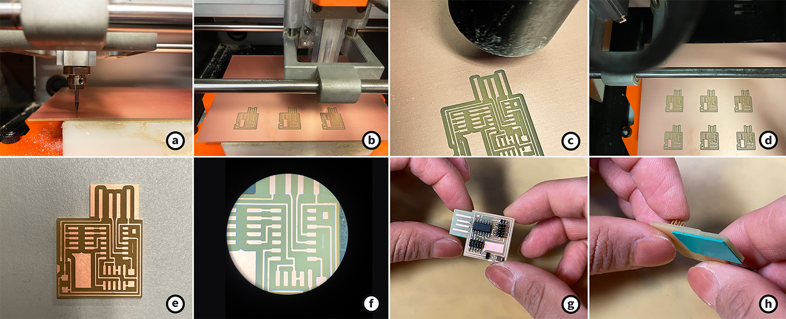
After determining the trace etching and board cutting settings, I went ahead working with the layout of the programmer board we were assigned to fabricate this week. Together with Wedyan and Simeon, we worked on a single-side copper coated plate of 15x8cm to etch and cut a total of 6 boards (2 per person). The traces looked neat and well defined, and the cut was quite clean likely due to using a fresh end mill.
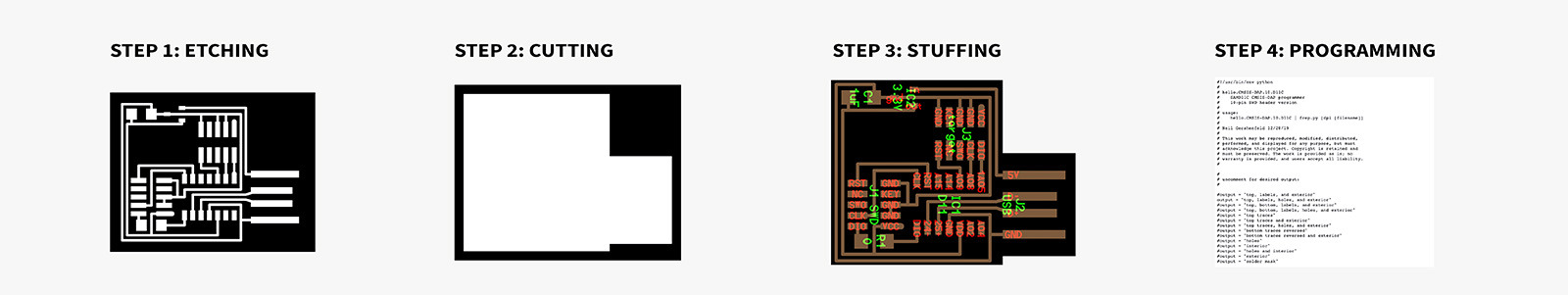
Step 1: Etching
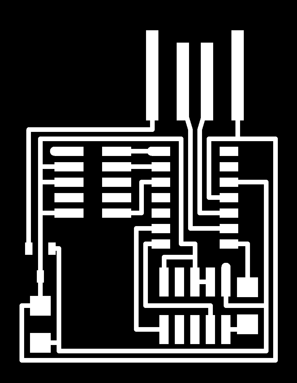
The first step was similarly to attach the plate to a flat and clean cutting bed using double sided tape. Next step was to fit the 1/64" end mill loosely to the head prior to setting the origin for etching (fig a). Using MODS interface, we set the origin to the part of the plate which would reduce the amount of waste material, but also provide us enough distance to etch and cut later. The Z axis was set at 8 mm, afterwhich we dropped the end mill to touch the copper plate and jammed it in place using the allen key. Once this step was complete, we uploaded the hello world traces .png file to MODS for etching the conductive traces and let the machine do its magic (fig b). Once etching was complete, we vacuumed the dust and particles (fig c).
Step 2: Cutting
For this step, the plate should be kept in place while changing the end mill to the 1/32" thick one. Once the end mill is changed, a similar process of recalibrating the origin is conducted. Then, the hello world interior .png file for the cut file is uploaded to MODS and the PCB is cut according to the design. Once the cut process is complete (fig d), the fairly larger particles and dust are vacuumed once again before taking the plate off the machine bed.
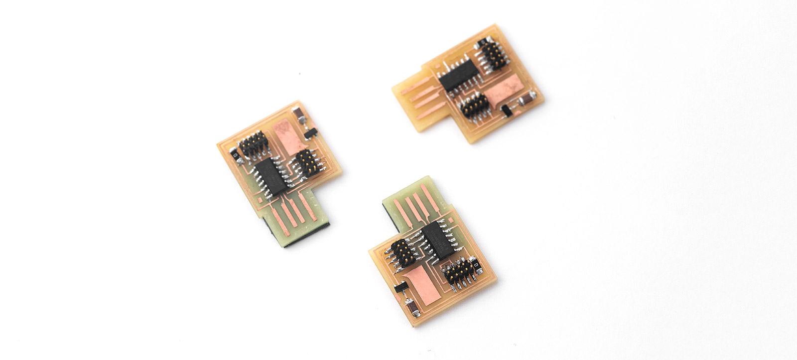
2.2 Stuffing the Board
Before stuffing the board with the surface mount parts, we had to clean up the excess traces on the board, near the USB insert, to avoid any shorting. We did that carefully using a doctor's blade or a knife (fig e). Before soldering parts, we checked the traces under the microscope to make sure there were no unwanted connections across the pads (fig f). After that, we soldered the surface mount components from center -> out. The components soldered are as follows; the ATtiny44 microchip, two 2x5 pin male headers, a 1 µF filter capacitor, a 0 ohm resistor (as jumper), and a voltage regulator (fig g). I did not use the microscope for this step as the pads were large enough to work with bare eye, however the light from the microscope helped. I also used double sided tape to stabilize the board while soldering. In this process, my best friend was the flux to keep the solder on the pads clean and shiny without any unwanted interconnects.
2.3 Programming the Board
Before programming, we needed to add some height using 3 layers of a single sided electrical tape to the (J2) USB to ensure contact of the conductive pads (fig h). With a completed board, the next step was to upload the firmware to turn this board into a programmer (fig i). We used a pre-written firmware and the EDBG programming utility to program the board through an Atmel programmer.
We used the following command: edbg -b -t samd11 -pv -f free_dap_d11c_mini.bin
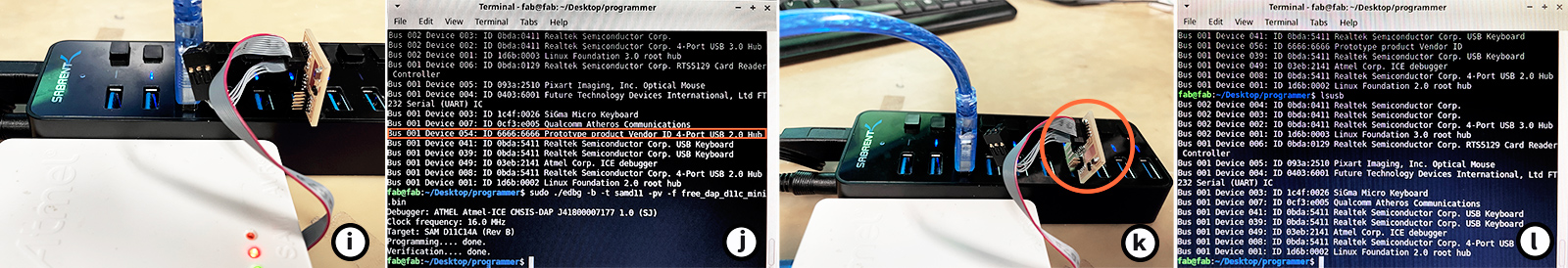
The board successfully programmed (fig j), and I was able to test it by removing and reinserting the board in the usb hub (fig k,l).
BONUS PROJECT: FLEXIBLE PCB
As an additional challenge, Wedyan and I decided to fabricate a flexible version of the Hello World board. And it wasn't easy!
3.1 Tracing and Cutting on Cricuit
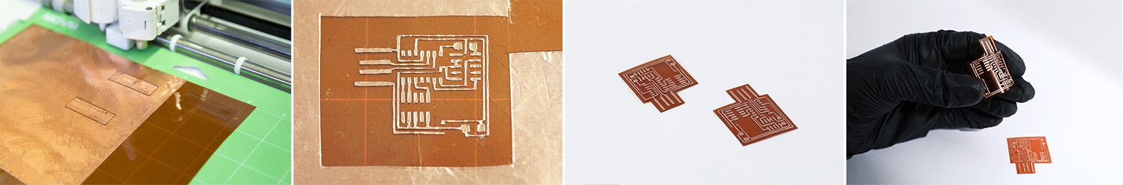
Our idea was simple - likely simpler than the milling process. We borrowed some adhesive copper tape with 20 cm width from the CBA shop to adhere onto a 300 micron thick polyamide sheet which we had in our lab. We would then upload the trace and cut .png files on Cricut Smart 2, which proved to be quite a decent equipment from last week's assignment.
Step 1: Adhering Copper Tape to Polyamide Sheet
We peeled the copper tape and slowly laid onto a flat sheet of polyamide (PAI). Since the adhesive layer is not too strong, we went over the composite sheet with a roller several times applying sufficient pressure. We ensured that there were no bubbles left and the copper adhered well to PI all over, as this would be crucial during the cutting process for the copper not to lift off of the PAI sheet.
Step 2: Tracing and Cutting
For this step, we had to configure a couple of parameters. First, we had to ensure that the size of the .png layers were similar to the real-life size of the board. Due to the dpi of the .png files, we had to manually resize the files on Cricut software. Secondly, we had to ensure that the tracing would only cut through the copper layer and not the PAI layer. For this, we went through several settings and finally settled on the "vinyl" setting as this provided a clean cut of the copper while not causing any knife traces on the PAI as desired. We then ran the interior cut layer once again to get the final flexible PCB board design.
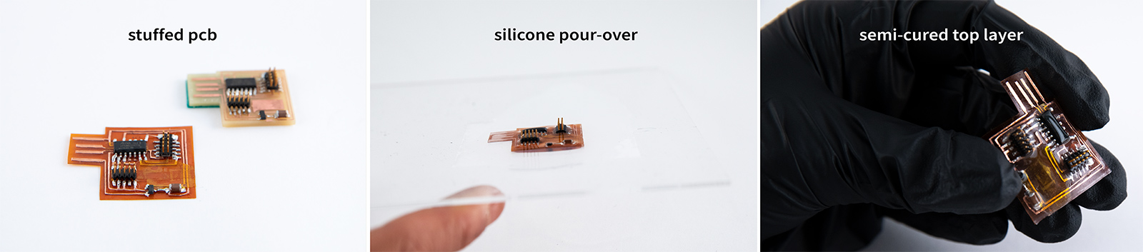
3.2 Stuffing the Board
This step was by far the most challenging as we ruined one of the boards due to the heat introduced by the soldering iron melting the adhesive layer of the copper, hence lifting of the copper traces from the PAI sheet. This destroyed all of our traces and the board design.
As a precaution, we added some reinforcing adhesive layers on the top, especially to keep the "floating" traces in place. For this, we used a 2mm wide polyamide tape and semi-fixed the traces in place before adding any solder onto them. This significantly improved the soldering of parts without having any issues with the traces being lifted off of the PAI. We finally succeeded with a fully stuffed flexible PCB as can be seen in the below image.
3.3 How to Bake Almost Anything: Silicone Top Layer
We removed the reinforcing polyamide tapes from the surface of the PCB carefully and poured a fast-curing silicone (Ecoflex-30A) which is compliant enough not to introduce additional stiffness to the flexible PCB. This helped both keeping the traces and components in place. As we did not want to insulate the USB traces, we masked these traces with an easy to remove tape before pouring the silicone over the board. For faster curing, we baked the composite board in the oven at 60°C for 30 minutes.
Once the silicone top layer was cured, we carefully cut the excess silicone that dissipated outside of the flexible PCB boundaries. However while doing so, we realized that parts of the silicone did not cure and we suspect that this is due to the flux left underneath inhibiting the silicone from curing. So, we left it over night to cure and we will see what comes out of it tomorrow and if our hypothesis is true. With all that, even though we could not test our board, we came a step closer to making a flexible PCB using a cheap Cricut machine and definitely see where we can improve our process such as better adherence between the copper and PAI layer, cleaning of the flux before pouring the top layer, and surely testing the connections before going any further with the top layer :)