INTRODUCTION

Two weeks ago, we learned about how to mill a PCB. This week, it is time for us to try out designing the schematic ourselves. We gained skills for designing a custom PCB, programming and testing the output. The assignment is two-fold as usual; an individual assignment where we design a board using our preferred software (Eagle in my case), trace and cut a pcb using MODS, stuff with components abd uploading the programmer, and the group assignment where we characterize and test the PCB (e.g. connections)
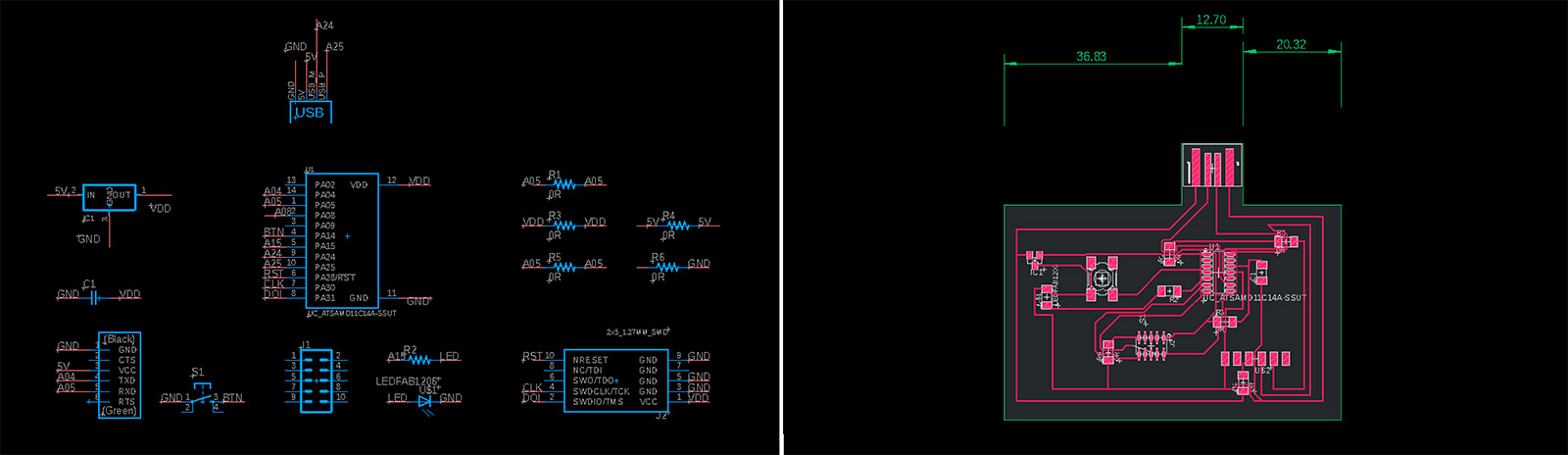
I used Eagle for drawing the schematic and generating the components' footprint since I'm already a Fusion user. The first step was to locate all the parts I wanted to use in the fab library. For future reference, the wonderfully unintuitive names of all the parts I used are as follows. Parentheses indicate subfolder names.
- Microcontroller: UC_ATSAMD11C14A-SSUT
- Voltage Regulator: VR_REGULATOR-SOT23SOT23 (VR_REGULATOR-SOT23)
- Button: SW_SWITCH_TACTILE_6MM6MM_SWITCH (SW_SWITCH_TACTILE_6MM)
- LED Diode: LEDFAB1206 (LED)
- Unpolarized Capacitor: CAP_UNPOLARIZEDFAB (CAP_UNPOLARIZED)
- Resistor: R1206FAB (R)
- 2x5 Connector: CONN_05X2SHD_SMD (CONN_05X2)
- 1x6 Connector: CONN_06_FTDI-SMD-HEADER
- USB Connector: CONN_USBPCB (CONN_USB)
INDIVIDUAL PROJECT
1.1 Schematic Design
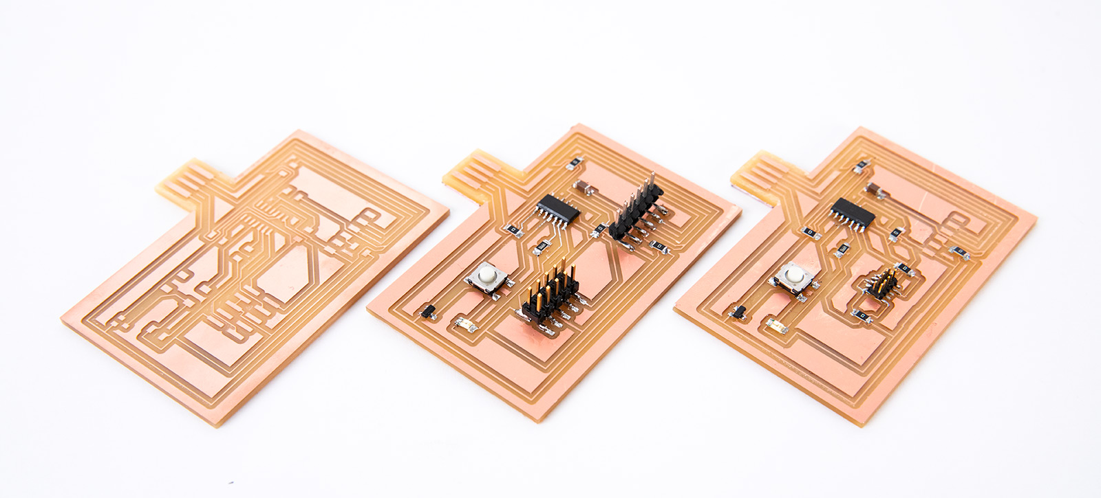
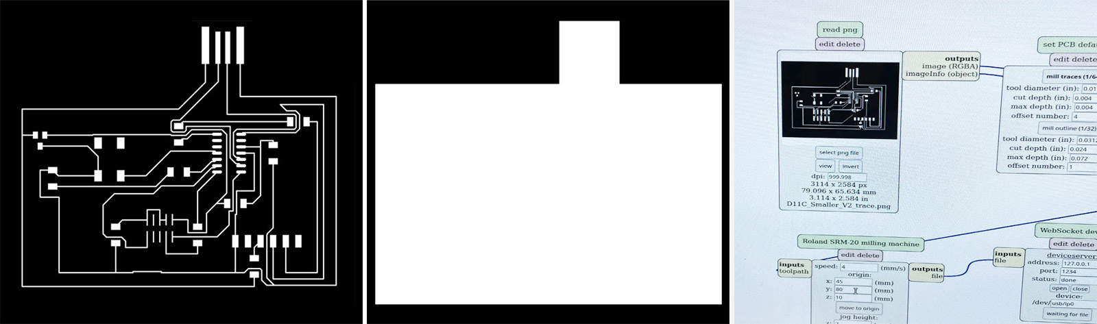
I referenced Neil's board designs (linked above) to determine which pins should be connected together, using the Week 3 board as reference for the connections for the 2x5 connector, which had 3 GND pins and pin 10 connected to VDD (3.3V). Pin numbering for microcontroller involves count the pins counterclockwise starting from top left. For the 2x5 connector, pins are numbered left to right, top to bottom. Additionally, we were asked to add at least one LED and one button to the basic board. After importing the libraries, it was quite easy to get the components added to the schematic. The most difficult part was to layout the footprint, where paths cannot cross. I spent ~3 hours tweaking and reconnecting, and it felt like a mental gymnastics. After I got everything connected, I cleaned it up a little and then realized there were some redundant components and wiring. The final footprint looks like below!
Handy Eagle Tips:
- The software will automatically connect wires for you if you drawing short wires from each pin and then name the connecting wires with the same name (I usually named them based on where the wire is going - i.e. a particular pin on the microcontroller or parts of the USB port). ;
- Naming wires GND automatically connects it to a GND pin;
- The order of the parts does not matter in the schematic (unless parts are connected in series):
- Renaming wires just involves selecting the "Change name of every segment on sheet" option.
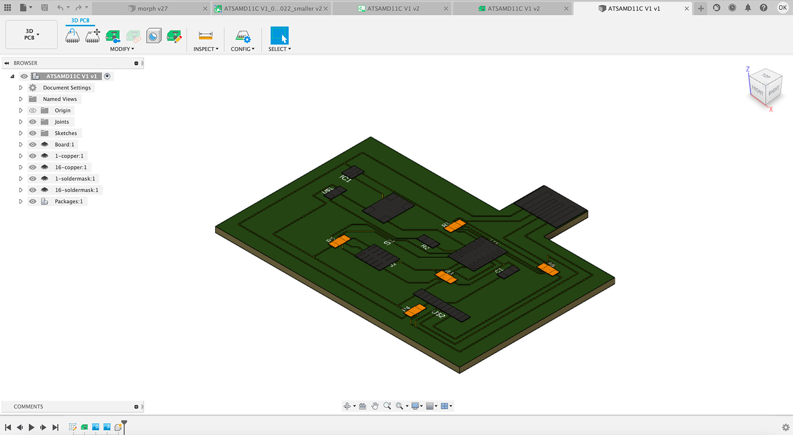
1.2 Board Design
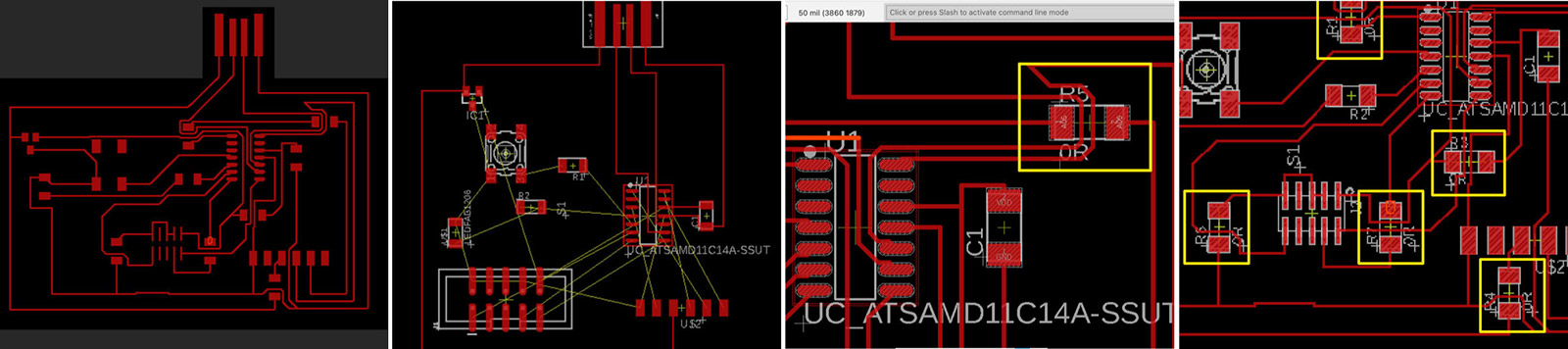
When it came to drawing traces, I just decided to go for it and mess around from scratch, instead of copying from a reference. The first step was placing all the parts on the board with the least amount of crossovers between the parts. I placed the voltage regulator in the top left of the board, given its USB connection. To connect the D+ and D- USB traces with some of the microcontroller pins, these traces went underneath the microcontroller, which can fortunately fit a total of three traces. For future board designs, I should prioritize these traces first. I also placed the capacitor as close to the microcontroller as possible, since its purpose is to provide the microcontroller with charge if there's a sudden demand. Rotating objects also helps out with the process. The alt key allows for more precise grid snapping. The default grid was more course and resulted in some angles in my traces and some wobbled lines, which I cleaned up at the end.
Notes on Settings:
- Set trace width as 10.
- For DRCs (design rule check), under Clearance, set all the top values (wire, pad, via) to 16.
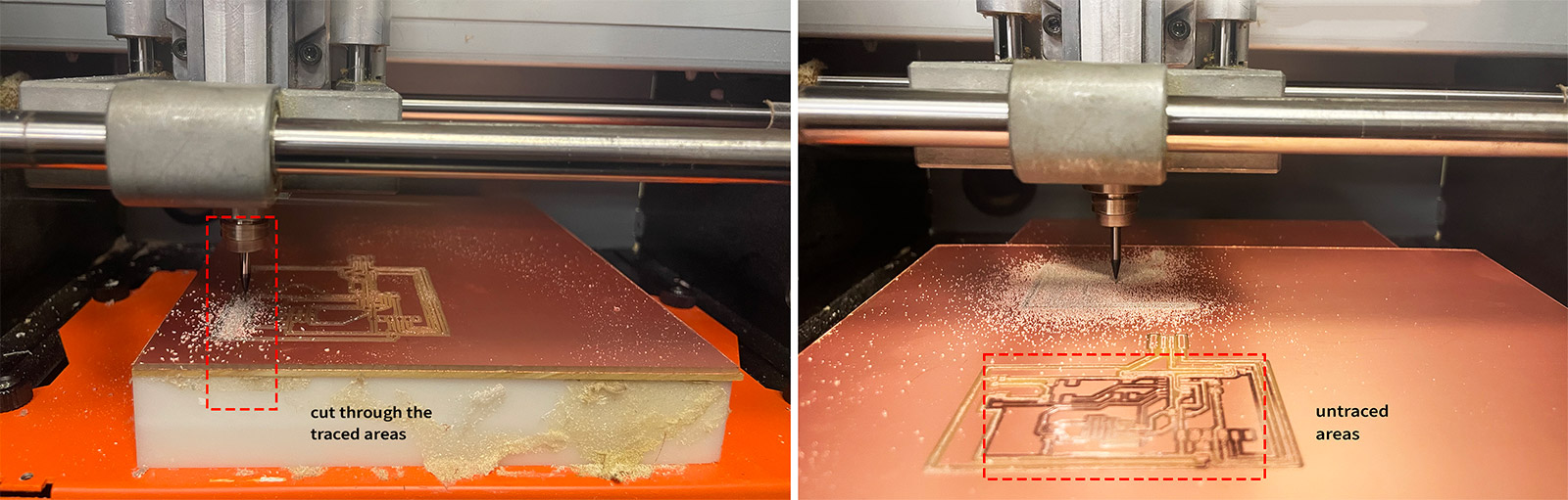
- The first issue was unmatching outline for cut and traces which resulted in cutting through our traced board.
- A second issue was having untraced areas that look shiny due to being slightly traced but not all the way through and we figured that this was because of the end mill being damaged (see figure below).
- A third and totally unanticipated one was due to the copper plate being too big, we could not calculate where it ended hence we went beyond the endmill's maximum boundary which resulted in having a portion of our board not traced or cut.
- A final issue, that we are still not certain of, is the bent copper board and thus not having even tracing all along.
- LED: orange. Black line indicates negative (to be connected to GND), green indicates positive.
- Microcontroller: SAMD11
- Voltage Regulator: 3.3 V 0.1 amps
- Capacitor: 1 microfarad Soldering went fast and smooth. I soldered all the small parts first roughly from inside to outside, then did the same for the large parts.
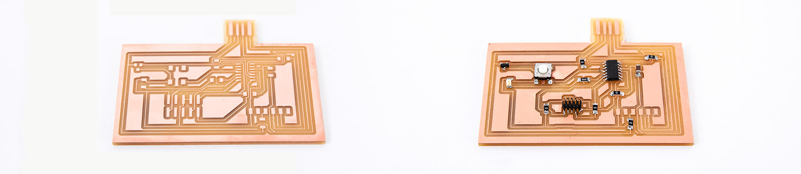
I made a few modifications to my schematic during the board design process. I swapped the pins that the LED and button were originally connected to, to reduce overlapping wires. I deleted the CTS and RTS connections to the microcontroller, since Anthony mentioned that we won't need them unless we are processing very large amounts of data. I also deleted the 10k resister by the LED since I accidentally connected it in series with the LED and microcontroller and because there is already a pullup resistor built in, though I'd need to program it in. Since a few bridges across traces were needed, I grouped together some traces and added four 0 Ohm resistors in my schematic.
Step 1: Milling
We exported the .png for traces on Eagle without any multistep process. However for the outline cut file we had to manually design the .png on Adobe Illustrator, based on the traces design. Once the export was complete, together with Wedyan, we worked on a single-side copper coated plate to fabricate two boards with slightly different components (2x5 header size).
The first step was to attach the plate to a flat and clean cutting bed using double sided tape. For ease of removal, we used the thicker double-sided tape in multiple sections of the board, every other 5mm, to keep it stable on the bed. Next step was to fit the 1/64" end mill loosely to the head prior to setting the origin for etching. Using MODS interface, we set the origin to the part of the plate which would reduce the amount of waste material, but also provide us enough distance to etch and cut later. The Z axis was set at 8 mm, afterwhich we dropped the end mill to touch the copper plate and jammed it in place using the allen key. Once this step was complete, we uploaded the traces .png file for etching the conductive traces and let the machine do its magic. Once etching was complete, we vacuumed the dust and particles. Then we uploaded the outline .png file and cut the board. Our board turned out to be quite big, but we decided that we will optimize the design once we finish the minimum viable for this week's assignment, so we left it as it is.
Milling Failures:
It was quite surprising to for all possible failures to occur in the process as in the Electronics Production week we had absolute 0 issue during the milling process. Hence, I will outline the error modes we experienced for others to learn from;
Step 2: Stuffing
Locating parts was a fun adventure. It turns out that the 2x5 connector in the fab library is not the exact same one as the one I used in Week 3 and is in fact bigger, which EDS fortunately had in stock.
Parts
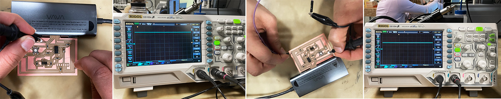
Step 3: Bootloading and Testing
Arduino we tested two modes; (a) switch on/off and (b) blinking light.
loaded the wrong bootloader to begin with (the mini, not generic) - then loaded the correct one but then both were loaded. it wasnt being recognized even if it said it was programmed and done. therefore, we ran the command that deletes the bootloader before (-e thingy) then uploaded the correct one. this solved it. https://fabacademy.org/2020/labs/ulb/students/quentin-bolsee/projects/samd11c_uart-updi/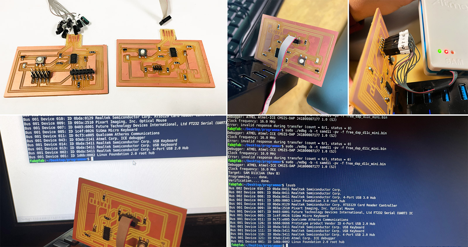
SAMD11C14 UART/UPDI programmer
board manager library downloaded (fab one) then you can see on the port and code on arduino whatever you want I open a terminal and run the following command to flash the device:
edbg -bpv -e -t samd11 -f sam_ba_Generic_D11C14A_SAMD11C14A.bin Pay attention to the -e parameter, which tells edbg to completely erase the memory before starting. This makes sure any previously installed bootloader gets removed. The output of the command should look like this:
Parts
Debugger: ARM CMSIS-DAP 1093000031387d241239333437353533a5a5a5a597969906 1.10 (S) Clock frequency: 16.0 MHz Target: SAM D11C14A (Rev B) Erasing... done. Programming................... done. Verification................... done. \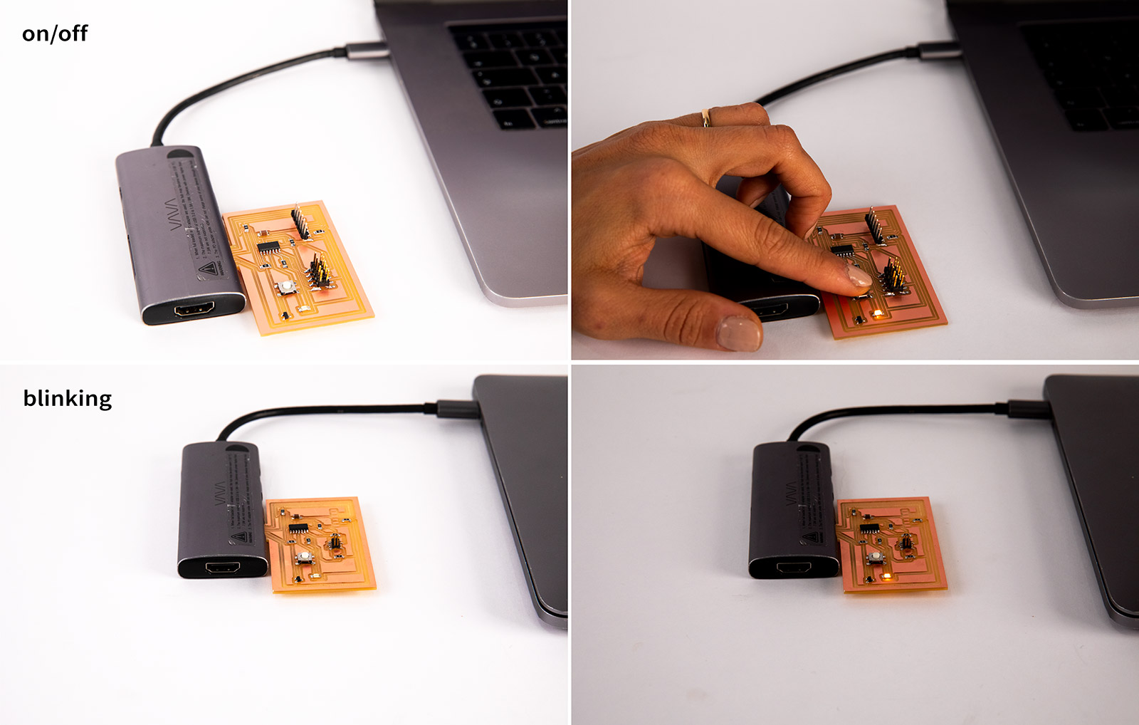
GROUP PROJECT
This week’s individual assignment was to fabricate Neil's "Hello World" board in-house, stuff it with electronic components and finally program it.
2.1 Testing the Board
After determining the trace etching and board cutting settings, I went ahead working with the layout of the programmer board we were assigned to fabricate this week. Together with Wedyan and Simeon, we worked on a single-side copper coated plate of 15x8cm to etch and cut a total of 6 boards (2 per person). The traces looked neat and well defined, and the cut was quite clean likely due to using a fresh end mill.
2.2 Programming the Board
Before stuffing the board with the surface mount parts, we had to clean up the excess traces on the board, near the USB insert, to avoid any shorting. We did that carefully using a doctor's blade or a knife (fig e). Before soldering parts, we checked the traces under the microscope to make sure there were no unwanted connections across the pads (fig f). After that, we soldered the surface mount components from center -> out. The components soldered are as follows; the ATtiny44 microchip, two 2x5 pin male headers, a 1 µF filter capacitor, a 0 ohm resistor (as jumper), and a voltage regulator (fig g). I did not use the microscope for this step as the pads were large enough to work with bare eye, however the light from the microscope helped. I also used double sided tape to stabilize the board while soldering. In this process, my best friend was the flux to keep the solder on the pads clean and shiny without any unwanted interconnects.
2.3 Blinking the LED
Before programming, we needed to add some height using 3 layers of a single sided electrical tape to the (J2) USB to ensure contact of the conductive pads (fig h). With a completed board, the next step was to upload the firmware to turn this board into a programmer (fig i). We used a pre-written firmware and the EDBG programming utility to program the board through an Atmel programmer.