Making an in-circuit programmer
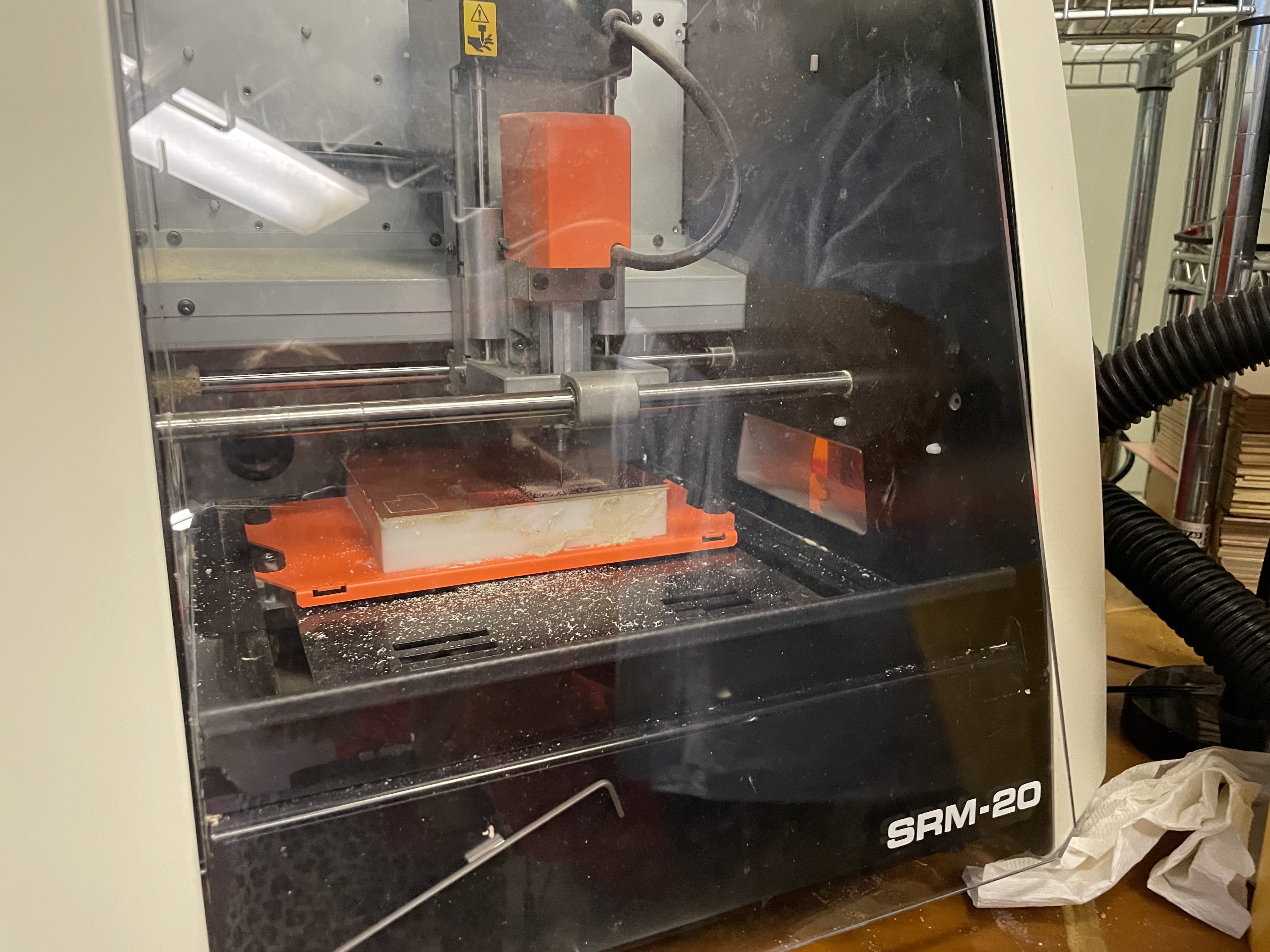
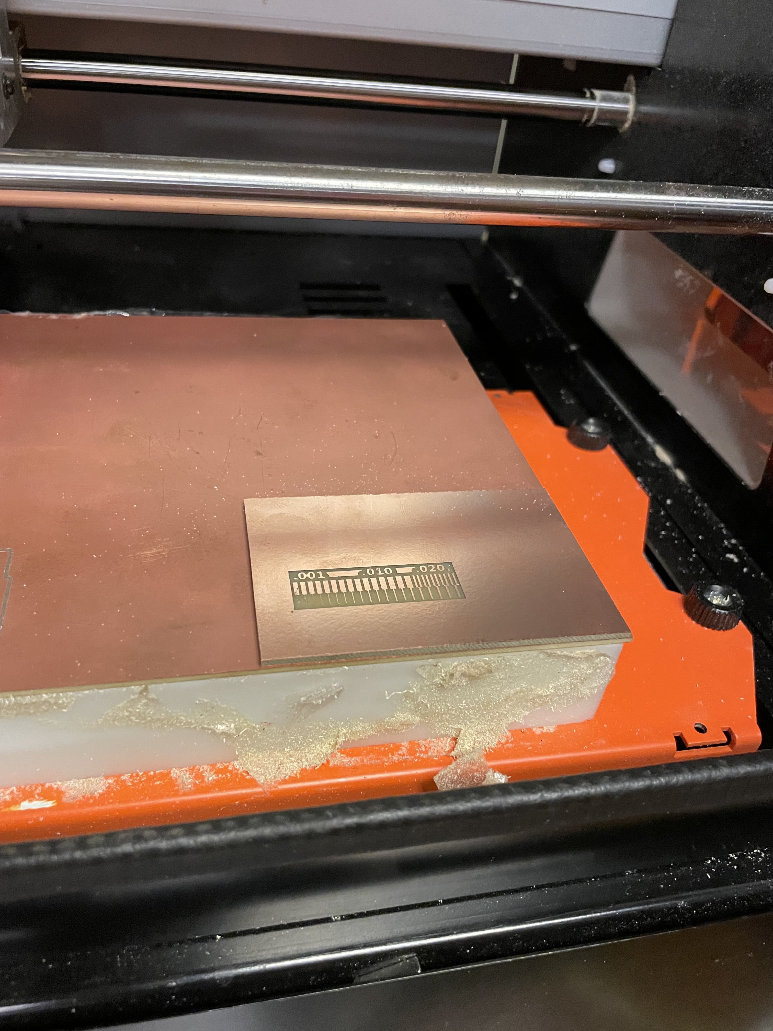
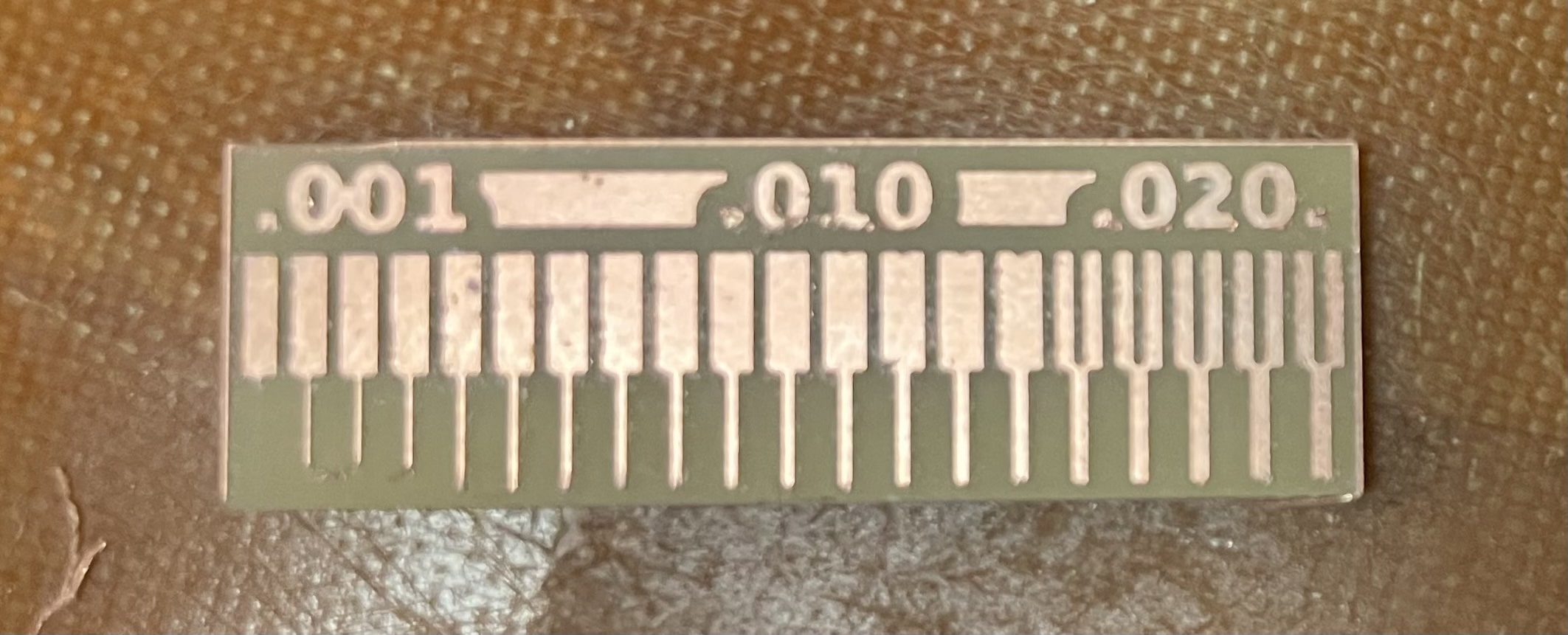
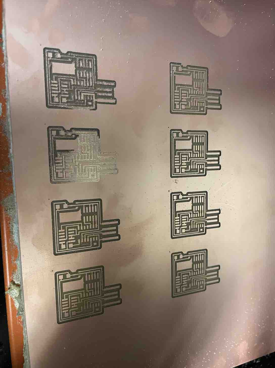
The first step of making the in-circuit programmer was to mill out the traces, then the outline of the Hello Board (USB-D11C-SWD-10 pin). I had previous milled out two of these boards, but due to inexperience with soldering such small parts, I ended up overheating certain joints and damaging the boards. I learned this final time when milling by milling 6 boards (for a total of 6 attempts should anything go wrong during the soldering process. At the end, I went through 4 additional boards before getting to a somewhat satisfactory result!) At first, when I milled traces using the 1/64th end mill, the traces were too shallow despite going through multiple callibrations. I changed out the end mill, and the traces finally got to the appropriate depth!
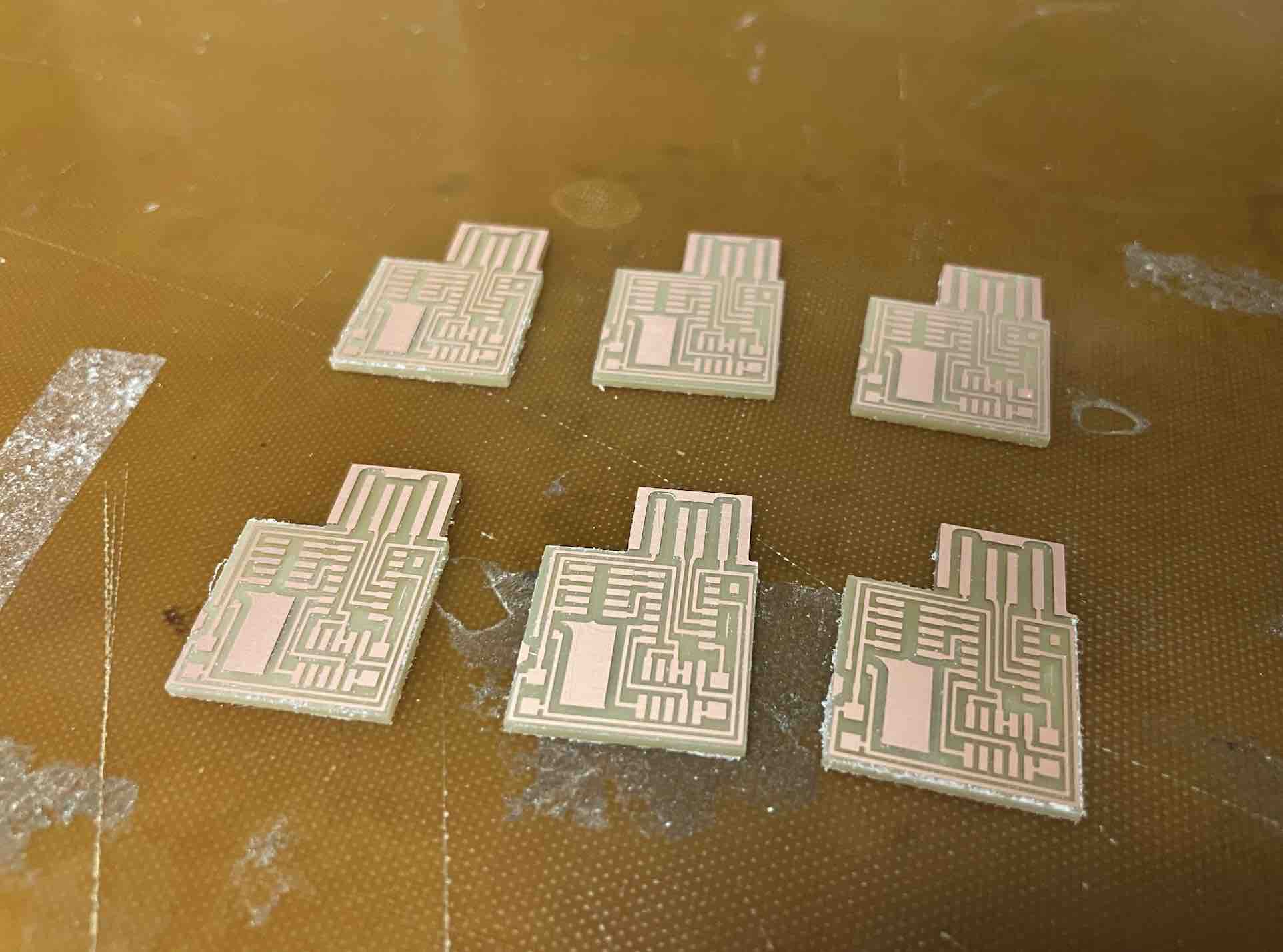
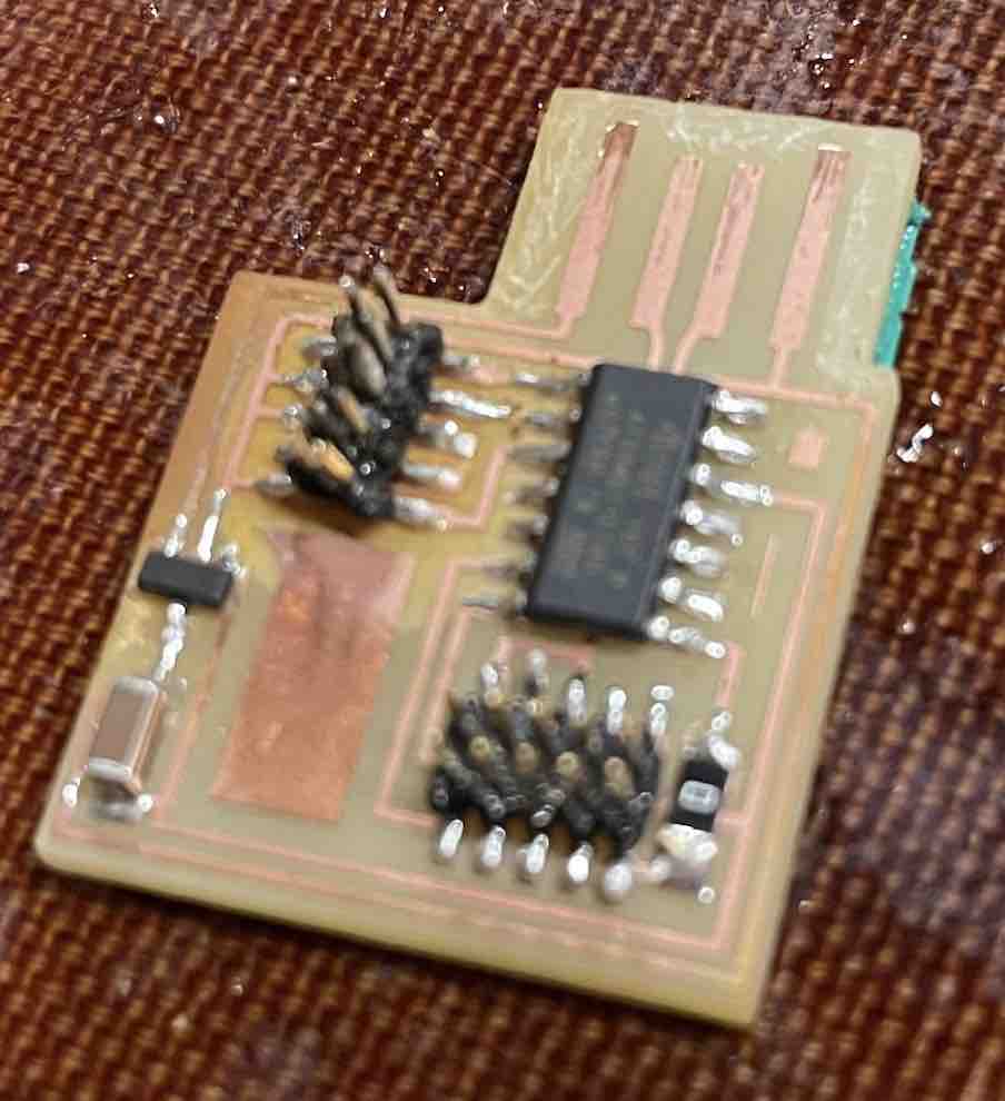
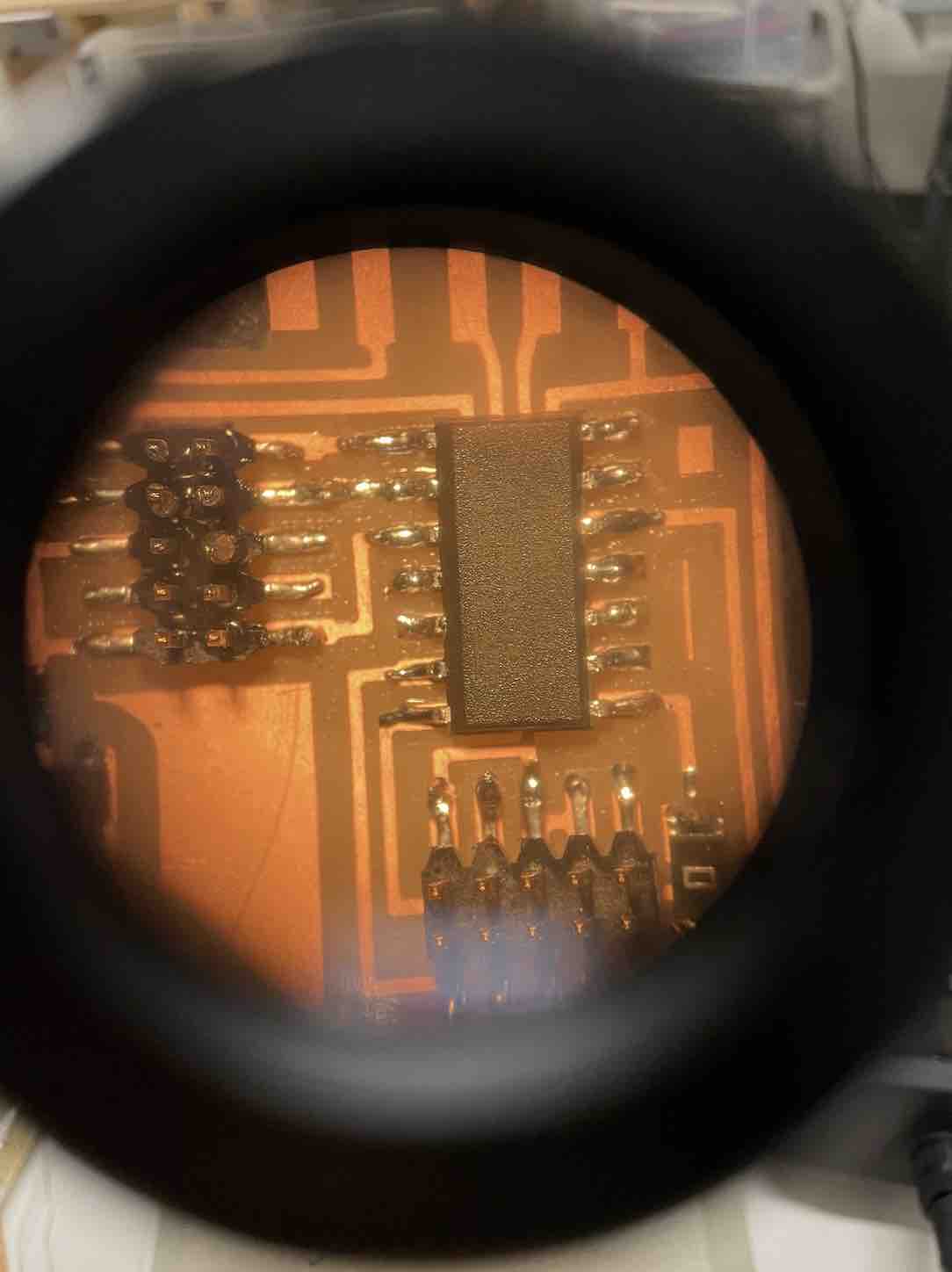
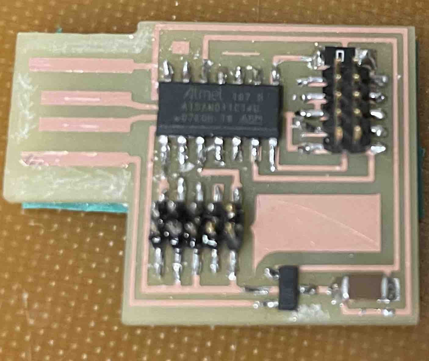
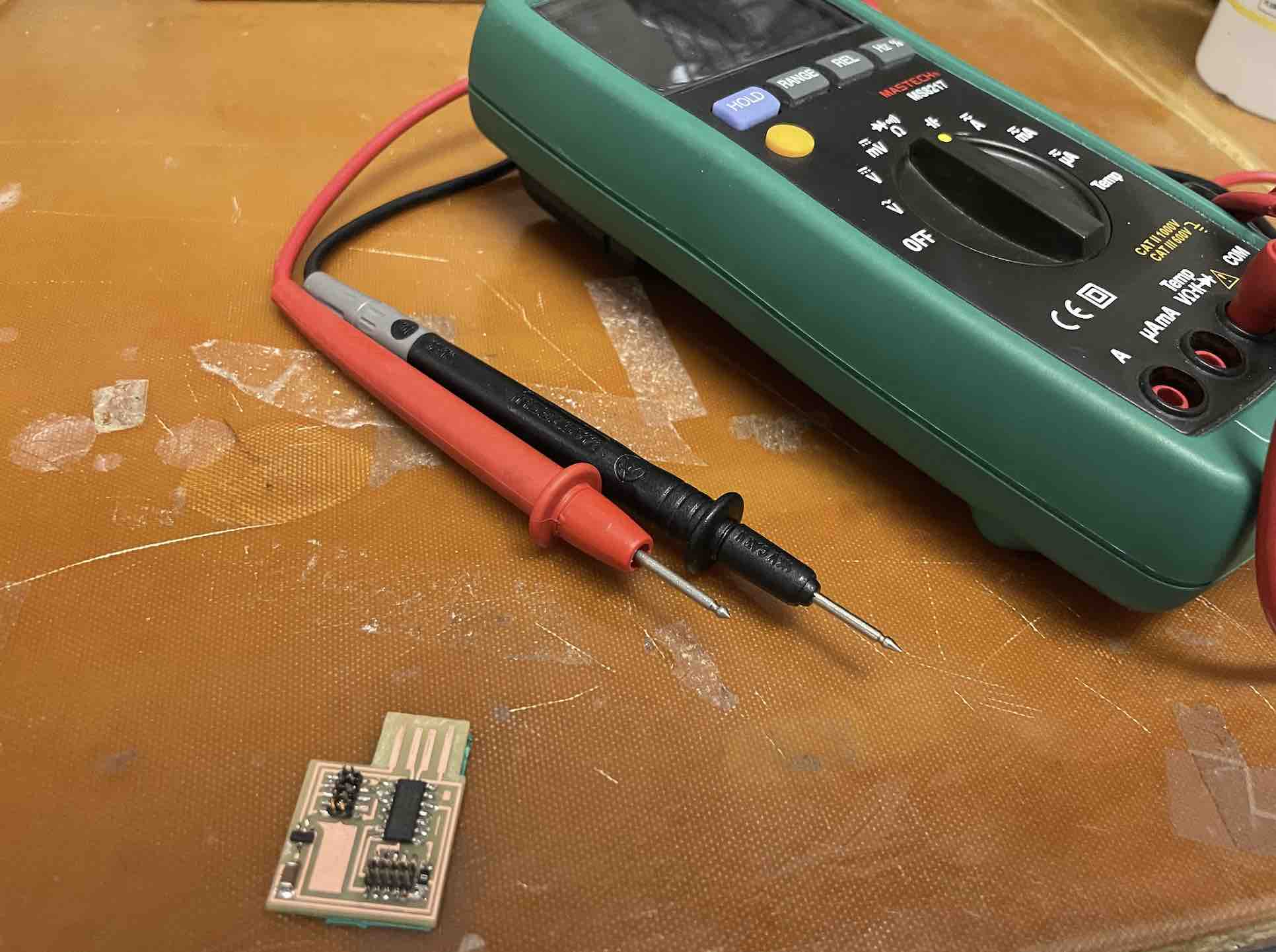
Then, I began the soldering process. Using lots of flux, the soldering wick/copper braid, and lots of attempts, I was able to get the board, shown below. I then placed lots of electrical tape underneath so that it could be inserted/fitted properly into a USB port.
When testing the board using the Hello script, I ran into issues where there was an invalid response during transfer.
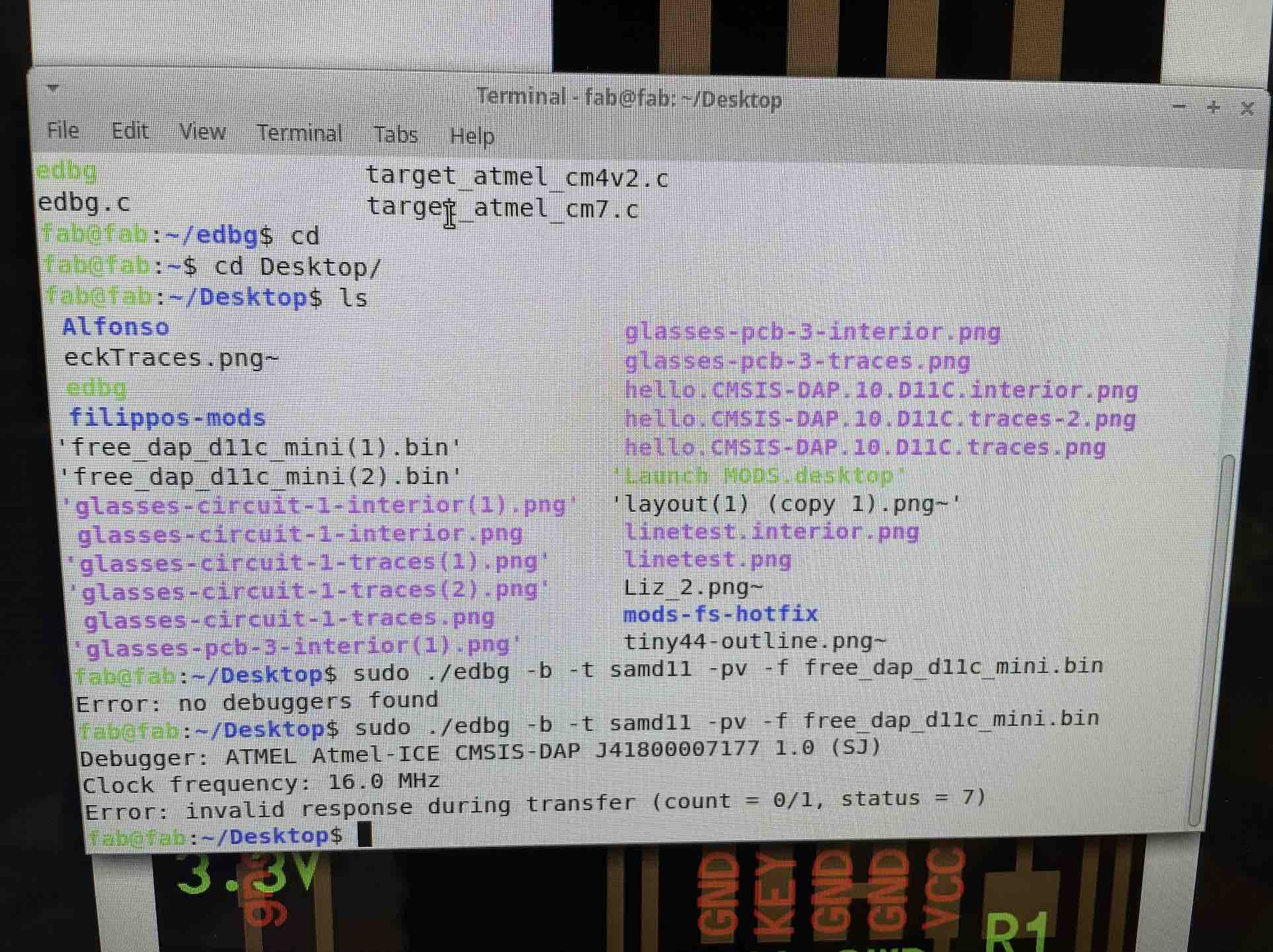
To debug, I tried flipping the orientation of the board (which resulted only in no debugger being identified by the terminal at all), then checked the status of all my joints using the short function of the multimeter. I checked that all the grounds and power (VCC, VDD) were connected and found that although they were, you had to press the probe of the multimeter on certain parts of each soldering joint to yield the short sound. I suspected that the reason the Hello code upload wasn't successful was because of weak joints that were inconsistent and depended heavily on orientation.
My next step was to reheat all the joints to reflow the solder using a heat gun. Unfortunately, I hovered the heat gun too closely and for too long over the board and one of the headers was damaged in the process.