(Group) Observe the operation of a microcontroller circuit board
(Individual) Redraw an echo hello-world board, add (at least) a button and LED
Check the design rules, make and test it.
(Group) Observe the operation of a microcontroller circuit board
(Individual) Redraw an echo hello-world board, add (at least) a button and LED
Check the design rules, make and test it.
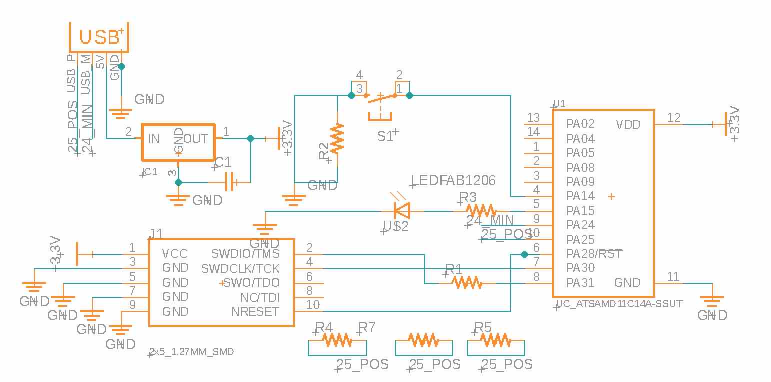
This week's assignment was challenging because of my inexperience with PCB design and layout. I began by going through Jake's MTM tutorial in Fusion to familiarize myself with the relevant commands. I chose to use the ATSAMD11C14A board because during the previous electronics production week, I had also used an SAMD11 and was used to the soldering sizes. I was worried that if I used a tiny board, then the soldering process would be much more tedious.
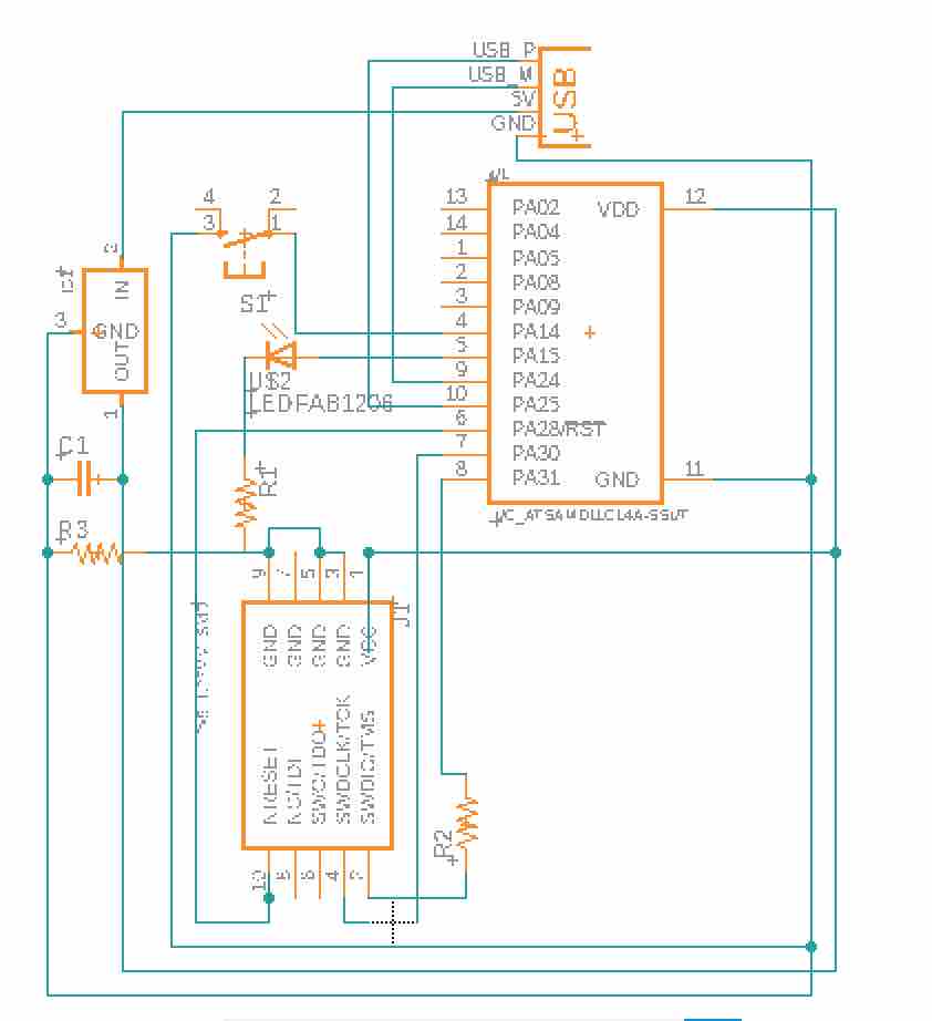
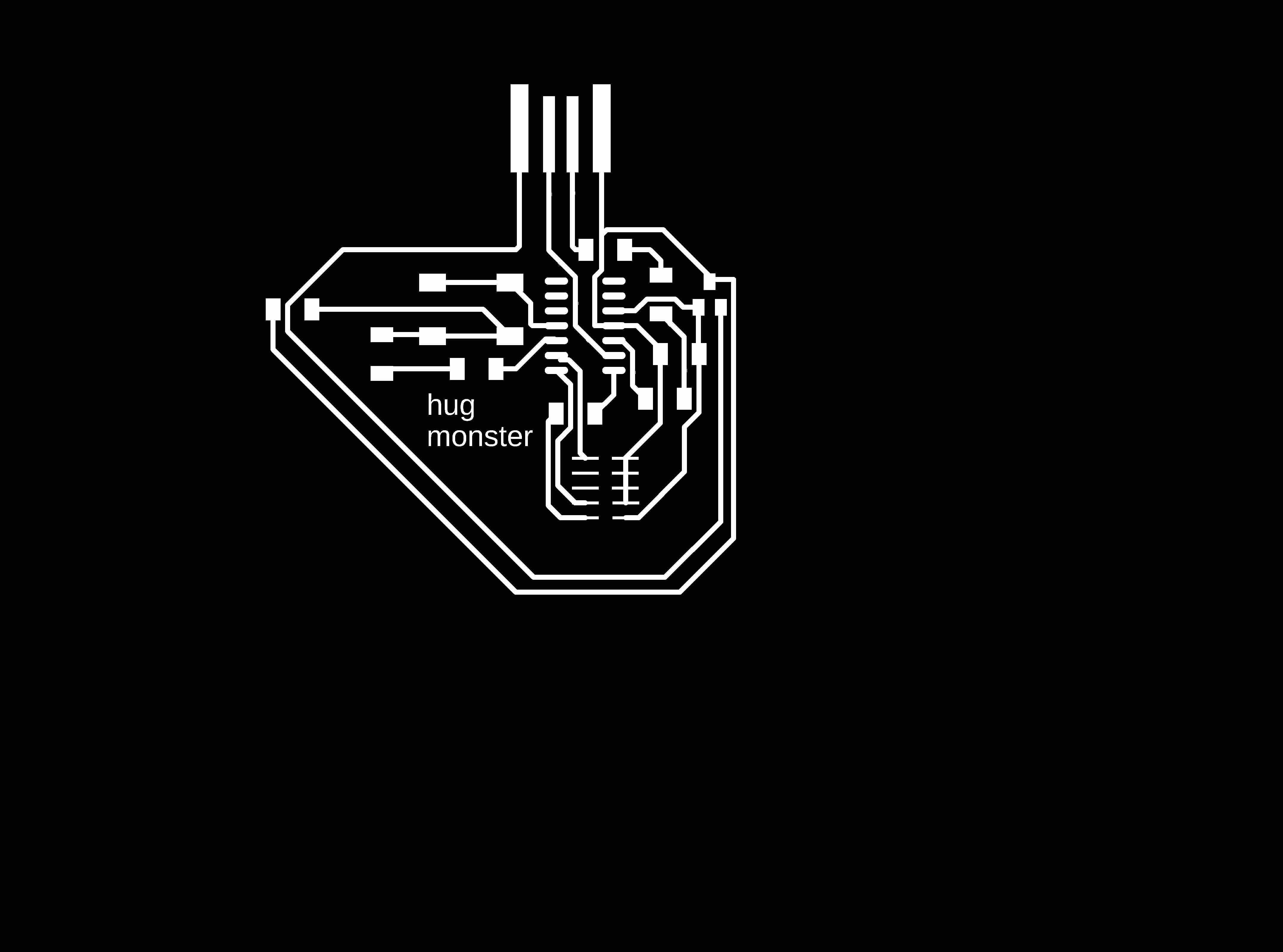
During the design process, I essentially followed the Echo hello board on the HTMAA website, while checking using the datasheet which available pins were Digital Input/Output. These pins were PA14 and PA15, so I used them to connect a button and an LED with a current limiting resistor.
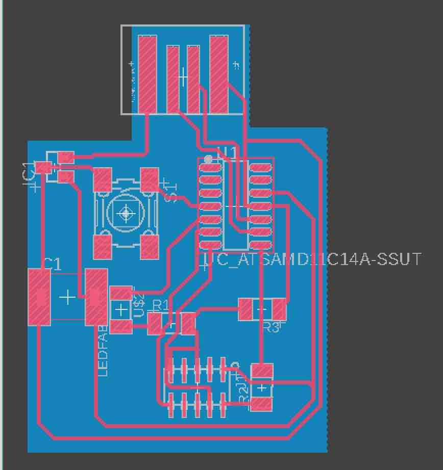
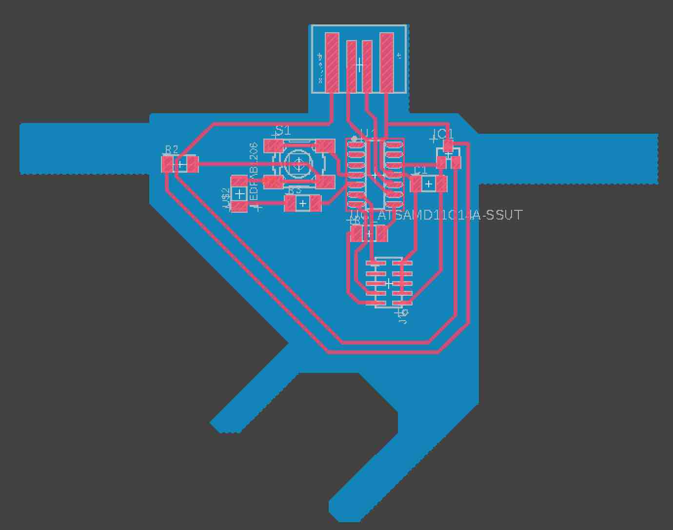
The layout was much more challenging than I expected. Within my design rules check, I had my clearance tolerances around 16 mm, but this ended up being way too large since it disallowed for any traces in the space between resistors and ICs which meant that I had to either use many more 0 ohm resistors or reduce the clearance tolerances. I chose the latter.
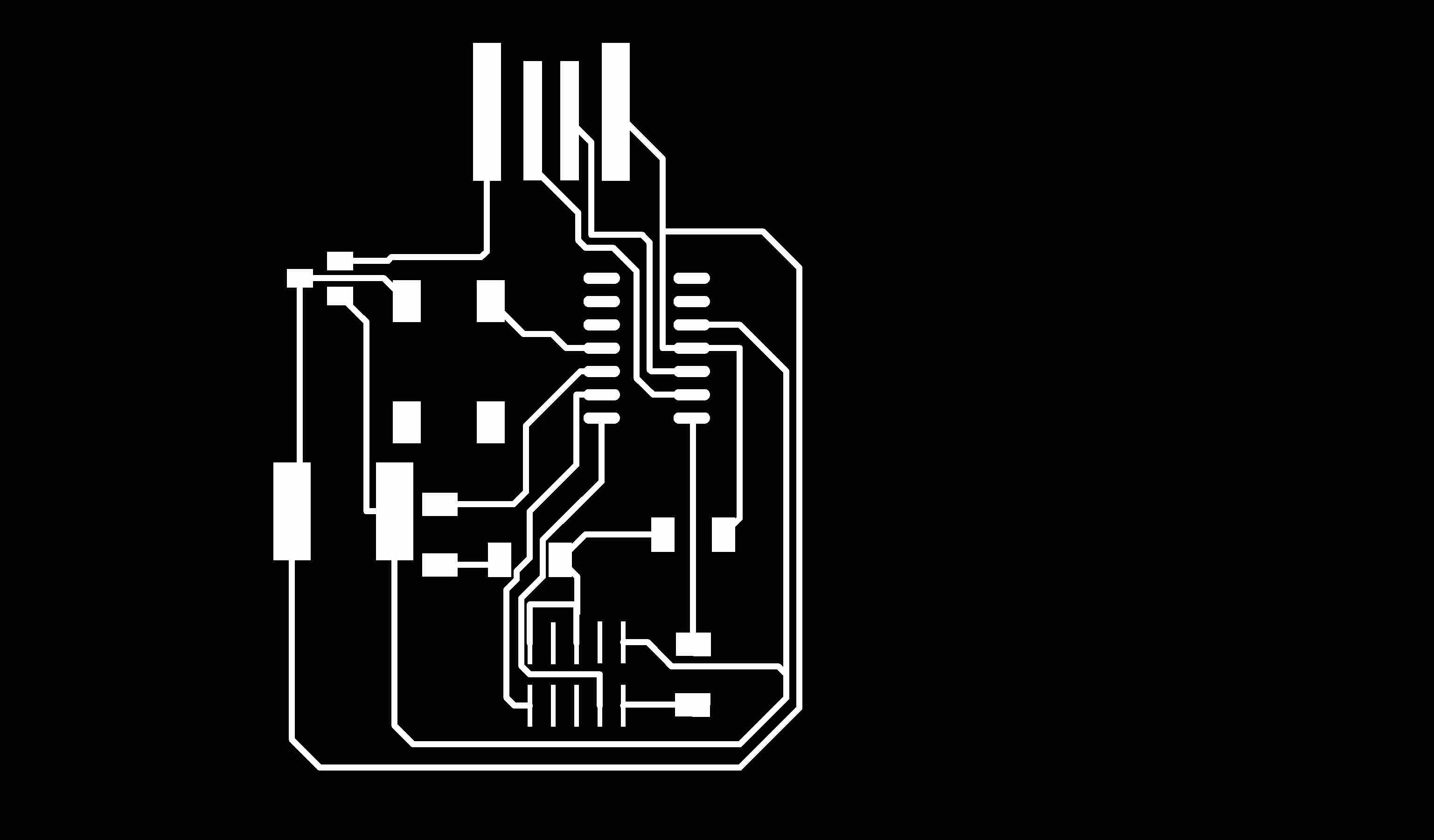
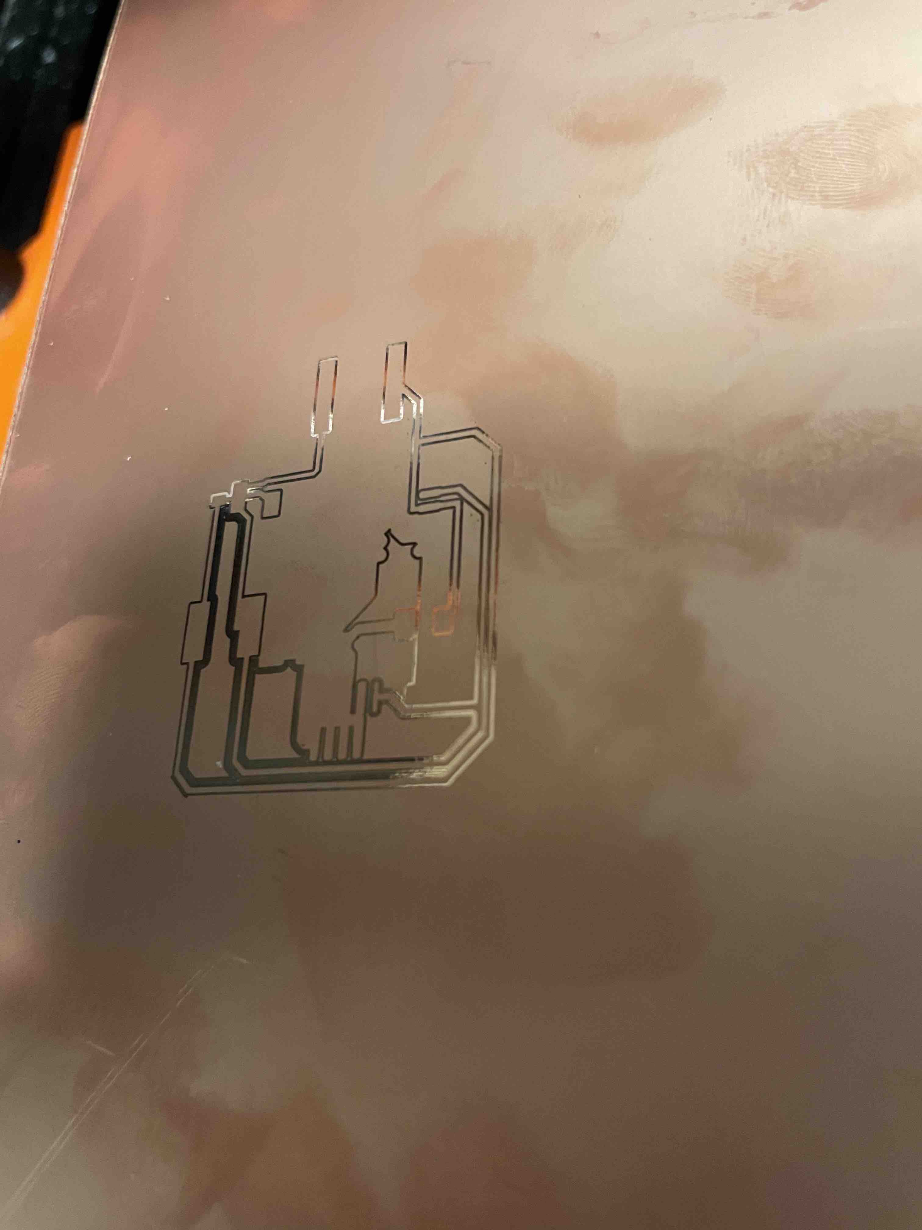
After much pain and adding one additional 0 ohm resistor, I came to the following PCB layout:
I finished by adding a polygon pour on the bottom layer so that I could get an outline when exporting to PNG for milling using mods.

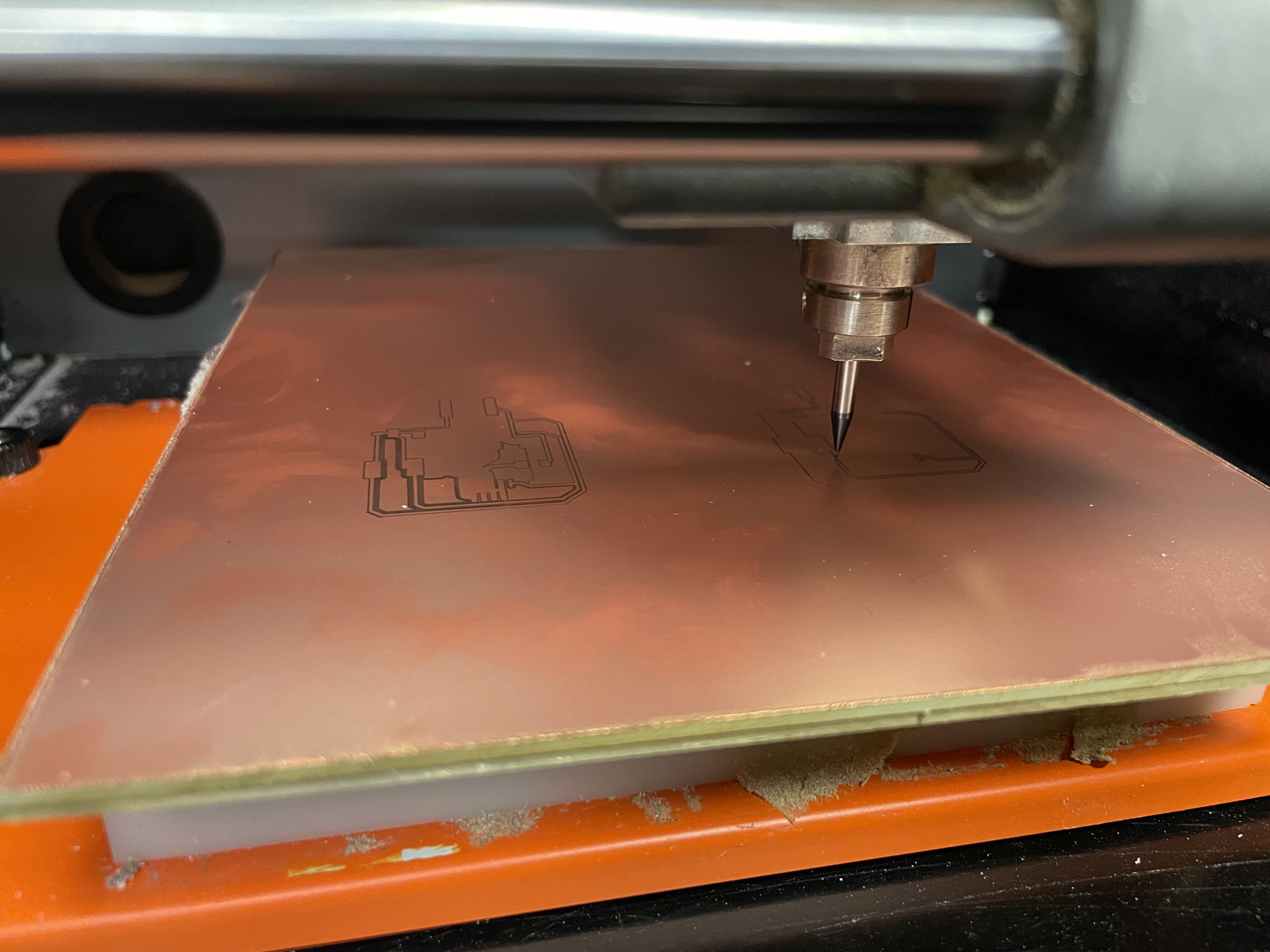
When I began milling, I ran into a significant challenge. The end mill was not cutting deep enough. I changed out the 1/64 end mill, recallibrated/loosened then tightened the end mill, and even restarted the machine, but was unable to resolve this.
I learned from a classmate in my class that in order to clean up the schematic and make the process of routing more clear (besides just following air wires), using nets to name power lines and GND was a good idea. Thus, I took my milling error (the end mill not cutting deep enough) as an opportunity to clean up my entire design and layout into a more creative, more straightforward design.
When routing, I still used too many 0 ohm resistors, but as I continue to lay out more boards, I'll be able to manage this better and optimize the placement of parts.
From there, I began milling. After talking to Miana, I realized that the reason I was having issues previously with some parts of the board being milled to the correct depth and others being too shallow was because of improper taping to the sacrificial layer of the milling machine which caused for some surface unevenness. It was likely not the product of incorrect end mill screwing, but the product of imprecise taping. Thus, I removed all the previous tape backing and put on new double sided tape. I found that this was much more successful.
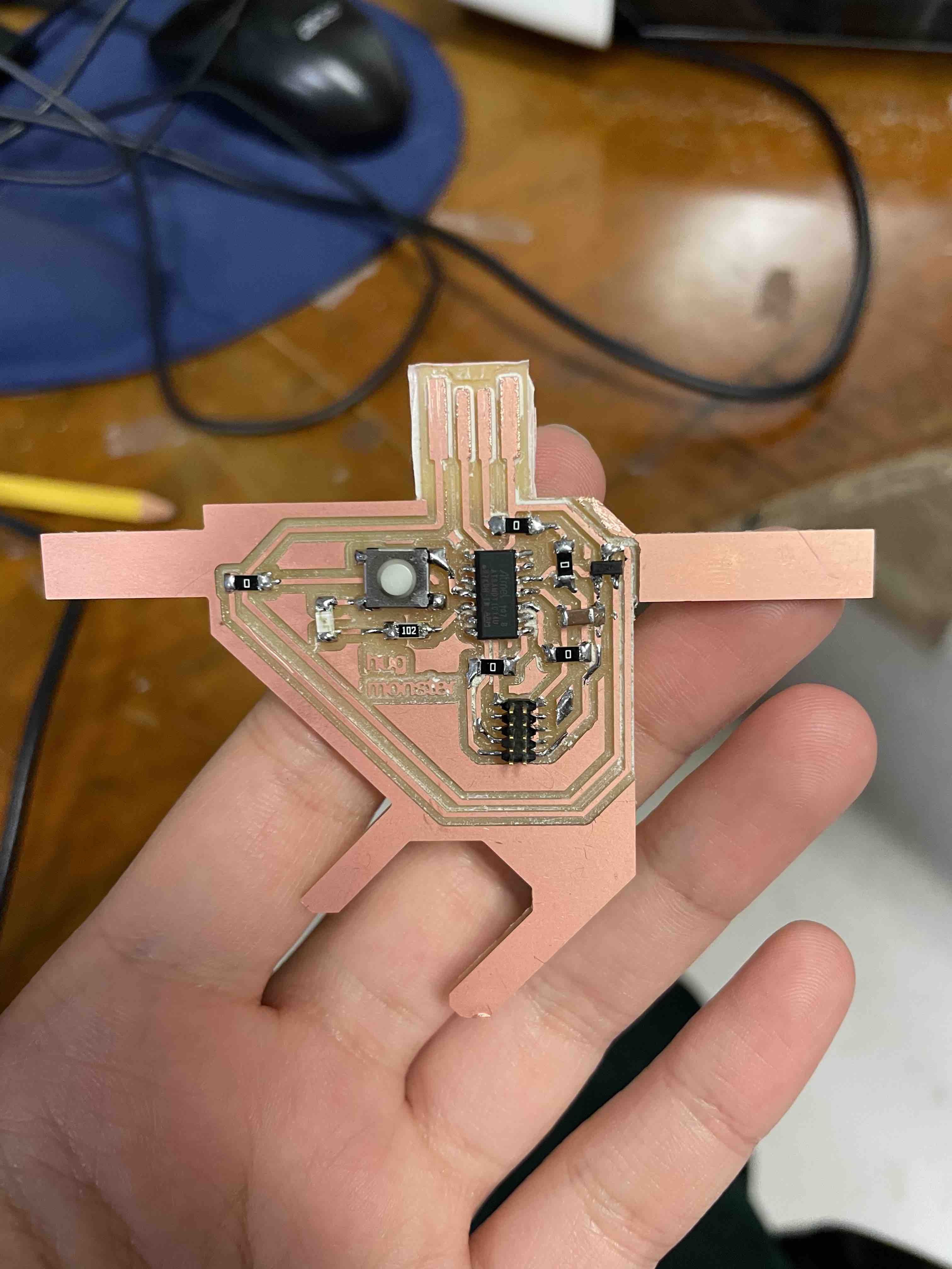
Next, I stuffed the board. This only took ~ 40 minutes as opposed to the painful 4 hour process from two weeks earlier. Progress! Knowing when the solder is flowing is the key to getting a quick and effective connection.
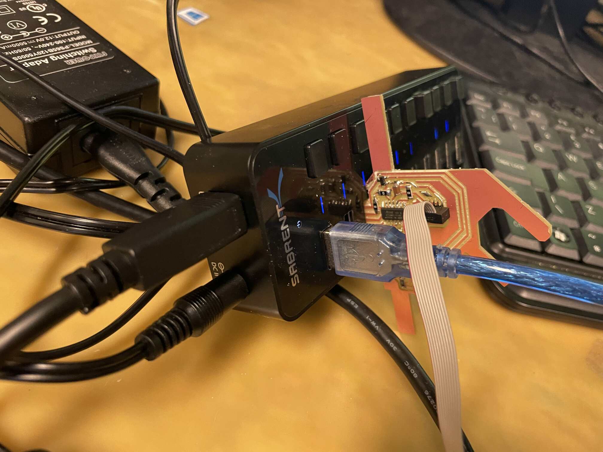
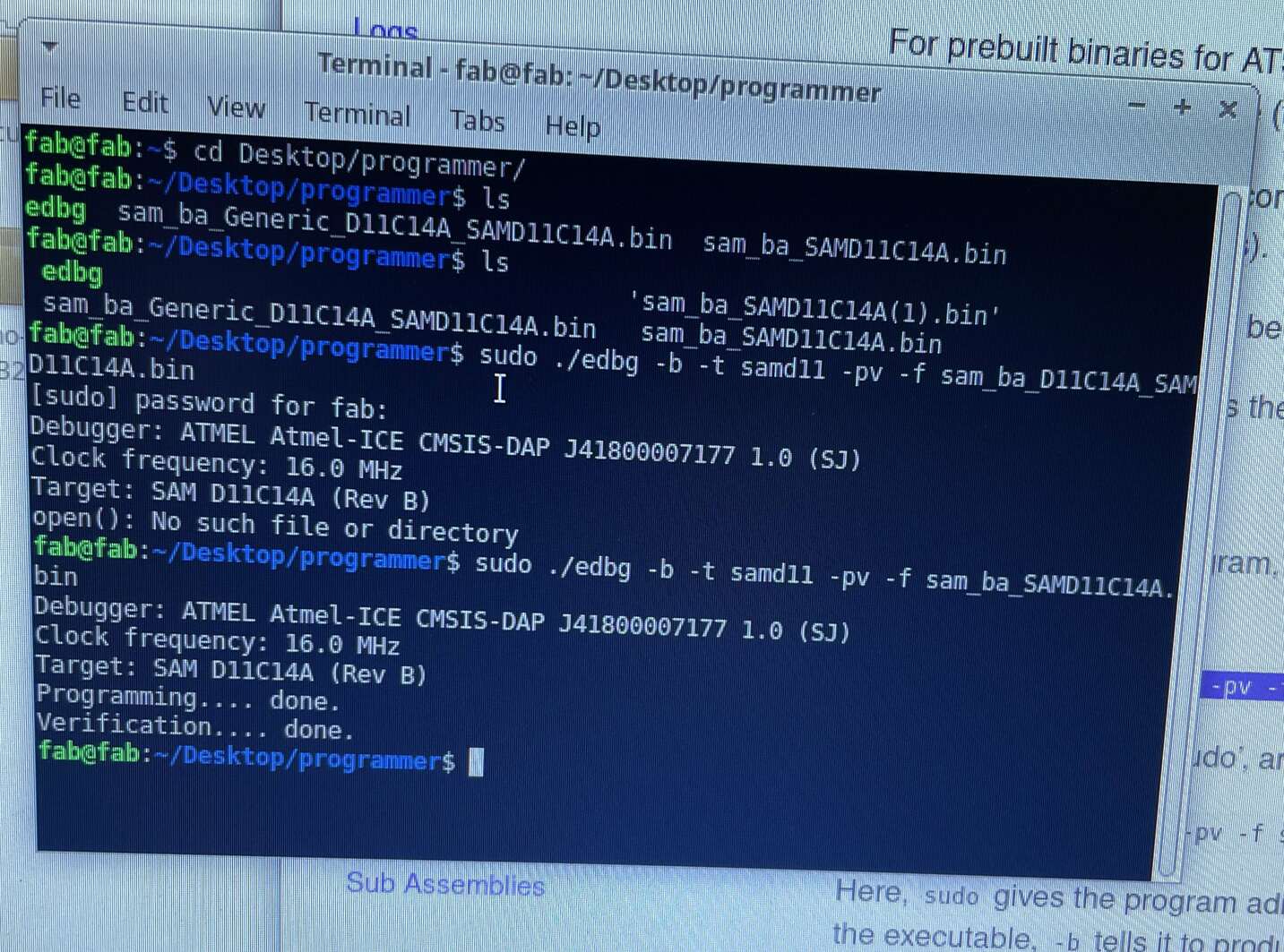
I then tested the connection with the SAMD and was able to get the board programmed! Success :)