Tools: Mods, PCB Milling, Soldering
Printed Circuit Board (PCB) Milling
This week, we learned about the different existing processes to fabricate printed circuit boards (PCBs). The assignment was to make an in-circuit programmer (USB-D11C-SWD-10) that includes a microcontroller using an in-house PCB production process (milling).
Production Process Characterization
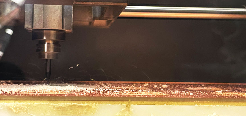
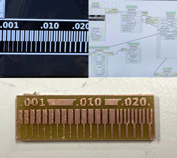
As a group assignment, we started characterizing the design rules for our in-house PCB production process using a Roland CNC milling machine. For this machine, a 1/64" end mill is used for traces, while a 1/32" end mill is used for cutting the board. We used modes, which was developed by Neil, as the computer-aided manufacturing (CAM) software to communicate with the CNC milling machine. We started with a test design in order to deterimne the thinnest traces the 1/64" end mill can successfully resolve. The traces test board can is shown on the right. To be safe, we decided to go with a trace width of 17 mills (0.4318mm).
Milling Process
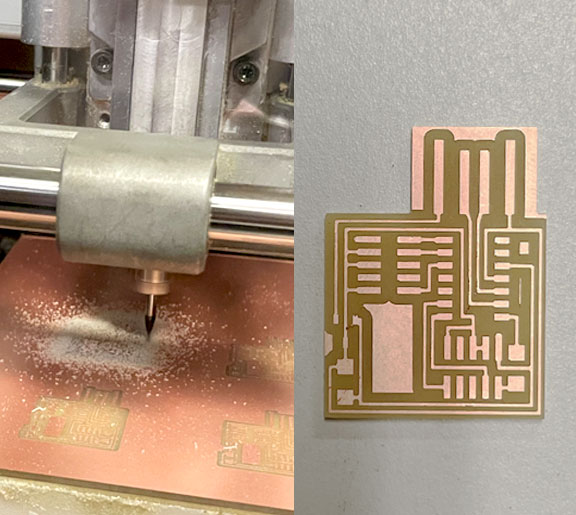
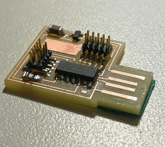
After determining the traces milling and board cutting settings, I uploaded the png file of the layout of the programmer board we are assigned to fabricate this week. The process of milling the board can be shown on the left, as well as the final produced board. The traces looked really good and well defined, and the cut was quite neat.
Soldering
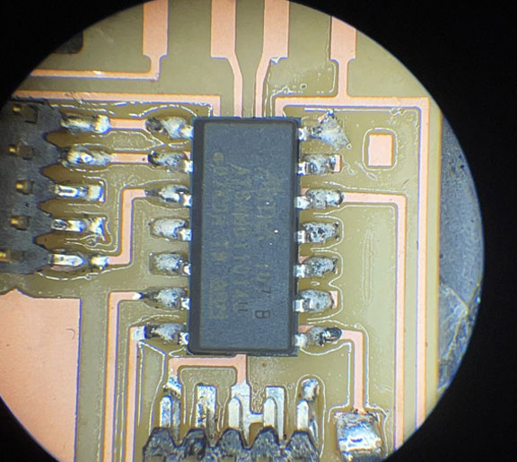
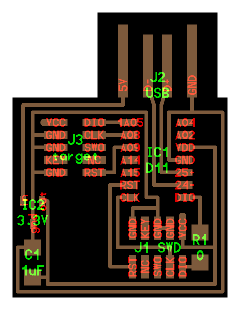
Now that the board with the patterned layout was fabricated, it was time to start populating it with the appropriate surface mount components. I collected the needed components at the CBA workshop. The programmer board itslef is quite minimalistic contianing the following components; a capacitor, a resistor, 3.3 V voltage regulator, the D11 microcontroller, and two JTAG headers. Afterward, I used the microscope and "a lot of flux" in order to facilitate the soldering process.
Failures and Debugging
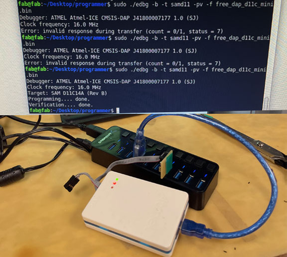
I fabricated two fully populated boards. One, I was able to get it programmed using The EDBG right away, thankfully! But, the other did not actually work!
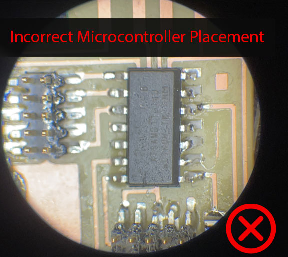
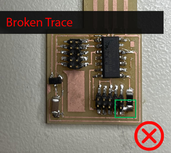
Below, you can find the terminal error message I was getting when I attempted to flash the second board. Thus, I embarked on a process to debug the issue existing with the second board. The first issue I discovered while inspecting the board under the microscope was that I had placed the microcontroller in the wrong orientation it was supposed to be (Oops!). To solve that, I used the hot air to take out the microcontroller completely with a tweezer and then flipped it to the correct orientation and soldered it again. After fixing this issue, I was fairly certain I would be able to program it. However, the error message showed up again! Next, I took our good old friend (the first line of defense for tracking down problems)and checked all my traces on the board. Unsurprisingly, I found a broken trace line connecting the zero ohm resistor with the JTAG header pin. Since the two components were close to each other, I just shorted it by using extra solder on that area to connect the solder joints as a quick solution.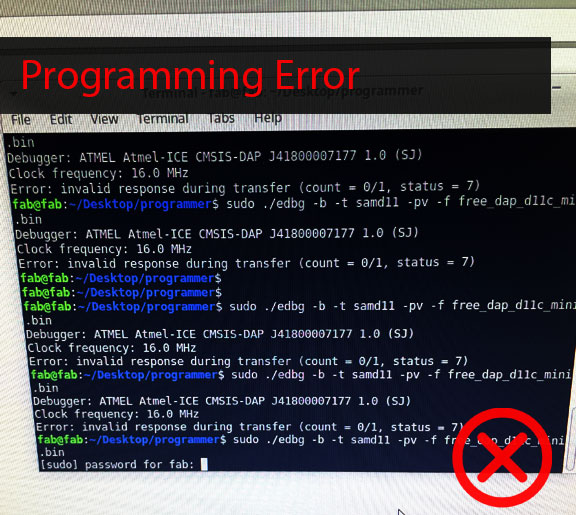
Finally it worked !
Luckily, after fixing the broken trace, the board actually worked!!
Board Programming
When I attempted to flash the board again, I was able to successfully program my programmer board, as shown in the terminal message on the photo! Here, it is a good practice to use a USB hub to avoid heating up the board too much when inserted directly into the computer
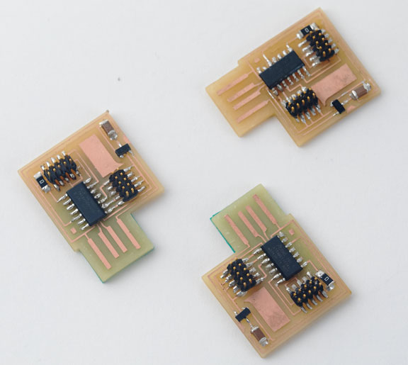
More Programmer Boards!
Previously, I mostly soldered components using the past and reflow oven. However, this assignment taught me how to improve and refine my motor control skills and be very, very, very patient!
Exploring other PCB Processes !
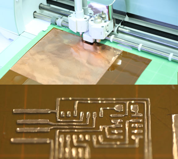
Inspired by Honghao Deng, My teammate Ozgun and I decided to try another process of fabricating flexible-substrate-based PCB using the vinyl cutter. We placed a piece of copper tape on top of a polyamide sheet on a flat mat. The objective was to cut the upper copper tape layer with the vinyl cutter and then slowly remove the extra copper areas during the process of weeding.
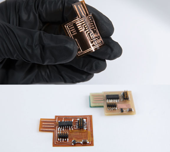
Flex PCB!
After a couple of trials, the process of fabricating the substrate itself went well. Although the traces' edges looked slightly deformed, all traces and pads were resolved without overlap/shorting between them. One issue though was the poor adhesion between the copper tape and the PI itself. We noticed while we were peeling it off; sometimes we needed to put a piece of tyape to keep it from not coming out. Soldering was even more challenging because the traces kept coming out. We also noticed that the fabricated pad footprints were slightly larger than the design, which is most likely a scaling issue while converting the file. After soldering, we casted a small amount of silicone to provide encapsulation. However, we still did not test if the board is working or not since we did not get the chance to program it yet. Programming and debugging this flex board is our next step!